Why is CVD preferred over PVD for high-aspect-ratio features? Superior Conformality for Semiconductor Fabrication
Updated 3 months ago
Chemical Vapor Deposition (CVD) is the industry standard for high-aspect-ratio (HAR) features because it provides superior conformality and step coverage. Unlike Physical Vapor Deposition (PVD), which is limited by "line-of-sight" mechanics, CVD utilizes gas-phase chemical reactions that occur simultaneously on all exposed surfaces. This allows for the uniform, void-free filling of deep trenches and narrow vias essential for modern integrated circuits.
Core Takeaway: CVD is preferred for complex semiconductor architectures because its chemical nature ensures uniform film thickness across 3D structures. While PVD suffers from shadowing effects in deep features, CVD achieves over 95% step coverage, making it indispensable for sub-10nm nodes.
The Mechanics of Superior Step Coverage
Gas-Phase Reactions vs. Line-of-Sight Deposition
PVD functions primarily through the physical transfer of atoms, behaving much like a directional spray that creates "shadows" in deep grooves.
CVD bypasses this limitation by using gaseous precursors that blanket the entire substrate. The film grows via a surface-controlled chemical reaction, ensuring that even the bottom and sidewalls of a deep trench receive a uniform coating.
Achieving High Conformality
In high-aspect-ratio features, maintaining a consistent thickness from the top of a feature to the bottom is critical.
CVD systems can achieve step coverage exceeding 95%, which prevents the formation of "keyhole" voids. These voids are structural defects that can trap impurities or lead to electrical failure in advanced semiconductor devices.
Precision Control in Advanced Fabrication
Managing Stoichiometry and Crystallinity
Beyond simple coverage, CVD allows for the precise regulation of gas flow ratios, furnace pressure, and temperature.
This level of control enables engineers to tune the chemical stoichiometry and crystal orientation of the thin films. Such precision is vital for achieving specific electronic functions in complex materials like MXenes or high-purity epitaxial layers.
Scaling for Sub-10nm Nodes
As integrated circuits scale down, the physical space for deposition becomes microscopic.
The ability of CVD to provide continuous, high-quality growth in these confined spaces is the primary reason it is used for scaling. Without the uniform film continuity provided by CVD, electrical performance and manufacturing yield would drop significantly at advanced nodes.
Stability and Material Efficiency
Higher Raw Material Utilization
CVD systems generally offer higher material utilization rates compared to PVD processes.
By directing precursors specifically to the reaction site, CVD significantly reduces waste. This efficiency is coupled with a simpler structural design in many tube furnaces, leading to lower long-term maintenance costs in high-volume manufacturing.
Thermal and Flow Field Stability
The stability of the thermal environment within a CVD reactor ensures ordered crystal growth over large areas.
Advanced configurations, such as cold-wall reactors, further refine this by heating only the substrate. This minimizes unwanted gas-phase reactions and prevents precursor decomposition on chamber walls, resulting in higher purity films.
Understanding the Trade-offs
The Thermal Budget Constraint
CVD typically requires higher temperatures than PVD to trigger the necessary chemical reactions.
This thermal budget can be a limitation when working with temperature-sensitive substrates or layers already containing metal interconnects. Engineers must carefully balance the need for conformality with the risk of thermal damage to the device.
Precursor Complexity and Byproducts
CVD relies on specialized chemical precursors that can be toxic, corrosive, or flammable.
Furthermore, the process generates chemical byproducts that must be effectively evacuated from the chamber using high-performance vacuum systems. Failure to manage these byproducts can lead to film contamination and reduced crystal quality.
Applying CVD to Your Fabrication Goals
Making the Right Choice for Your Project
Choosing between CVD and PVD depends entirely on the geometry and material requirements of your specific application.
- If your primary focus is filling high-aspect-ratio trenches or vias: CVD is the only viable choice due to its near-perfect conformality and void-free filling.
- If your primary focus is high-purity epitaxial growth for optoelectronics: Use Metal-Organic CVD (MOCVD) to achieve tailored compositions and low defect densities.
- If your primary focus is large-area 2D materials like graphene: Utilize a cold-wall CVD system to ensure uniform, single-layer growth with minimal impurities.
- If your primary focus is a low-temperature process for simple flat surfaces: PVD may be more cost-effective and safer due to the lack of complex chemical precursors.
By leveraging the chemical precision of CVD, manufacturers can overcome the physical limitations of traditional deposition to build the next generation of dense, high-performance electronics.
Summary Table:
| Feature | Chemical Vapor Deposition (CVD) | Physical Vapor Deposition (PVD) |
|---|---|---|
| Mechanism | Surface-controlled chemical reaction | Directional "Line-of-Sight" transfer |
| Step Coverage | Superior (>95%), highly conformal | Poor (suffers from shadowing) |
| Ideal Application | High-aspect-ratio trenches & vias | Flat surfaces & low-temp coatings |
| Fill Quality | Void-free, uniform 3D growth | Potential for "keyhole" defects |
| Thermal Budget | Higher (required for reaction) | Lower (physical process) |
Optimize Your Semiconductor Research with THERMUNITS
As a global leader in high-temperature laboratory equipment, THERMUNITS offers high-performance CVD/PECVD systems, Tube furnaces, and Vacuum furnaces specifically engineered for the precision required in material science and industrial R&D. Our solutions empower researchers to achieve superior film conformality and stoichiometric control across the most complex 3D architectures.
Our Thermal Processing Expertise Includes:
- Comprehensive Range: From Muffle and Atmosphere furnaces to Rotary, Hot Press, and Vacuum Induction Melting (VIM) systems.
- Tailored Solutions: Specialized Dental Furnaces and Electric Rotary Kilns designed for specific industrial demands.
- Precision & Efficiency: High-quality Thermal Elements and control systems to maximize material utilization and minimize waste.
Ready to overcome the limitations of traditional deposition? Contact THERMUNITS today to find your ideal thermal solution.
Mentioned Products
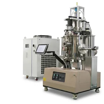
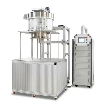
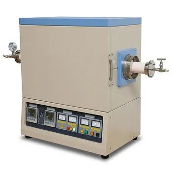
- Versatile Chemical Vapor Deposition Tube Furnace System for Advanced Material Research and Industrial Coating Processes
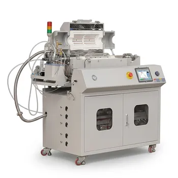
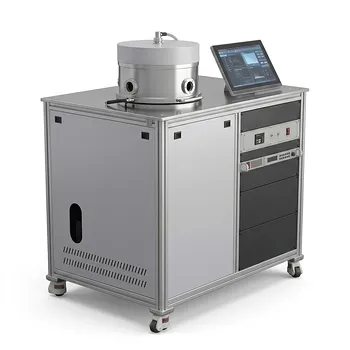
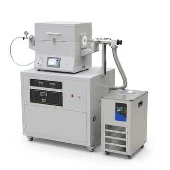
- Chemical Vapor Deposition CVD System Slide PECVD Tube Furnace with Liquid Gasifier PECVD Machine
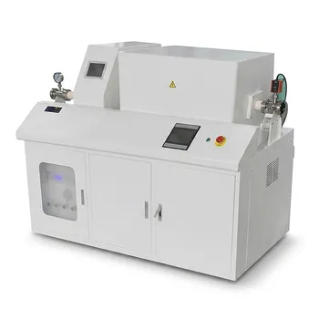
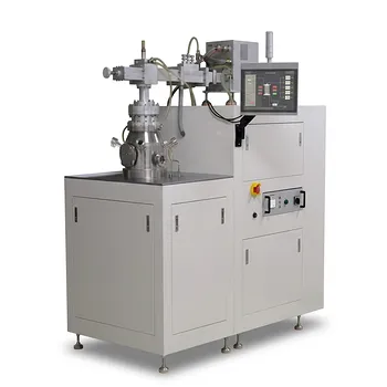
- Radio Frequency Plasma Enhanced Chemical Vapor Deposition RF PECVD System for Laboratory and Industrial Thin Film Growth
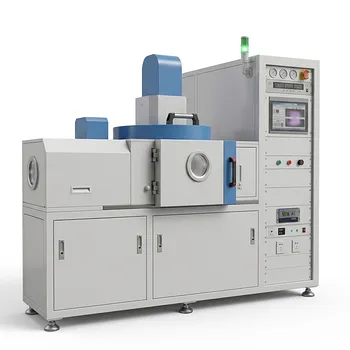
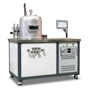
- 915MHz MPCVD Diamond Machine Microwave Plasma Chemical Vapor Deposition System Reactor
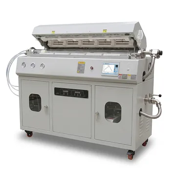
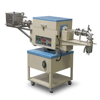
- Inclined Rotary Plasma Enhanced Chemical Vapor Deposition PECVD System for Thin Film Deposition and Nanomaterial Synthesis
People Also Ask
- What role do by-product desorption and evacuation play in CVD film quality? Key Factors for High-Purity Films
- What are the primary differences between hot-wall and cold-wall CVD reactors? Choose the Best System for High Purity
- How do temperature regimes influence the growth rate of films in a CVD system? Master CVD Kinetics for Superior Thin Films
- How does the deposition process occur within a Chemical Vapor Deposition (CVD) reactor? Explore the 5-Stage Growth Cycle
- How does a Chemical Vapor Deposition (CVD) system ensure product quality? Precision Control for 2D Nanomaterial Growth
Tech Team · ThermUnits
Last updated on Apr 14, 2026
Related Products
Versatile Chemical Vapor Deposition Tube Furnace System for Advanced Material Research and Industrial Coating Processes
Chemical Vapor Deposition CVD System Slide PECVD Tube Furnace with Liquid Gasifier PECVD Machine
Radio Frequency Plasma Enhanced Chemical Vapor Deposition RF PECVD System for Laboratory and Industrial Thin Film Growth
915MHz MPCVD Diamond Machine Microwave Plasma Chemical Vapor Deposition System Reactor
Inclined Rotary Plasma Enhanced Chemical Vapor Deposition PECVD System for Thin Film Deposition and Nanomaterial Synthesis
Cylindrical Resonator MPCVD Machine System for Microwave Plasma Chemical Vapor Deposition and Lab Diamond Growth
Multi Heating Zones CVD Tube Furnace System for Precision Chemical Vapor Deposition and Advanced Material Synthesis
High Temperature 1700C Dual Zone Tube Furnace for Material Science and Industrial Chemical Vapor Deposition Research
HFCVD Machine System for Nano Diamond Coating on Drawing Dies and Industrial Tools
Split Chamber CVD Tube Furnace with Vacuum Station Chemical Vapor Deposition System Machine
Two Zone Rotary CVD Furnace with Automatic Feeding and Receiving System for Powder Processing