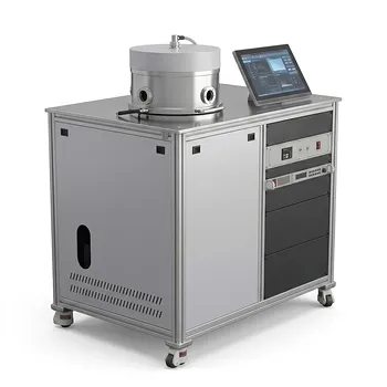
What are the primary technical variants and capabilities of CVD systems? Master High-Purity Material Synthesis
Updated 3 months ago
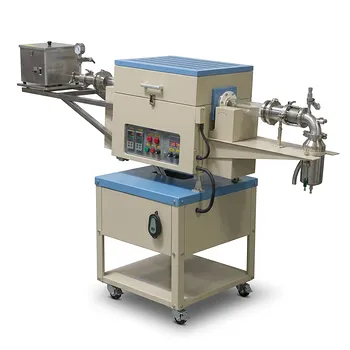
Chemical Vapor Deposition (CVD) systems are specialized instruments designed to grow high-purity solid materials via gas-phase chemical reactions on a substrate. The primary technical variants include Atmospheric Pressure CVD (APCVD), Low-Pressure CVD (LPCVD), Plasma-Enhanced CVD (PECVD), Metal-Organic CVD (MOCVD), and Chemical Vapor Infiltration (CVI). These machines enable the deposition of thin films, protective coatings, and nanostructures with nanometer-scale precision.
CVD systems represent the gold standard for achieving uniform, conformal coatings on complex geometries through controlled chemical reactions. By manipulating temperature, pressure, and gas flow, these systems allow for the precise engineering of a material's electronic, optical, and mechanical properties.
Core Technical Variants of CVD Systems
Pressure-Dependent Systems (APCVD and LPCVD)
Atmospheric Pressure CVD (APCVD) operates at standard pressure and is often used for high-throughput applications like protective coatings or simple oxides. While older systems were bulky, modern compact APCVD units can reduce the equipment footprint by over 50%, saving valuable cleanroom space.
Low-Pressure CVD (LPCVD) operates in a vacuum, which enhances the diffusion of gas molecules and significantly improves film uniformity. This variant is a staple in semiconductor manufacturing for growing high-quality polycrystalline silicon and dielectric layers.
Energy-Enhanced Systems (PECVD and MPCVD)
Plasma-Enhanced CVD (PECVD) uses electrical energy to create a plasma in the reaction gas, allowing deposition to occur at much lower temperatures than thermal CVD. This is critical for depositing films on temperature-sensitive substrates that would otherwise melt or degrade.
Microwave Plasma CVD (MPCVD) is a specialized variant used primarily for synthesizing high-purity diamond films. Because it operates without electrodes in contact with the plasma, it eliminates metal contamination, producing materials with superior thermal and optical clarity.
Precursor-Specific Systems (MOCVD and CVI)
Metal-Organic CVD (MOCVD) utilizes metal-organic precursors to grow complex crystalline layers, particularly for optoelectronics like LEDs and laser diodes. It offers exceptional control over the chemical stoichiometry and crystal orientation of the resulting thin films.
Chemical Vapor Infiltration (CVI) is a unique adaptation of CVD used to deposit materials inside porous objects or fiber preforms. This capability is essential for creating high-strength ceramic matrix composites used in aerospace and high-temperature industrial applications.
Key Capabilities and Performance Metrics
Atomic-Level Precision and Conformality
One of the most significant capabilities of CVD is step coverage, the ability to deposit a uniform layer even on deep trenches or complex 3D microstructures. This is achieved because the gas-phase precursors flow into every available crevice before reacting on the surface.
CVD systems also allow for targeted alloying and atomic-level deposition. By adjusting the concentration of secondary metal precursors, manufacturers can produce intermetallic catalysts with high phase purity.
Material Purity and Doping Control
CVD processes facilitate in-situ doping, where impurities are added directly during the growth process to alter the electrical properties of the film. This is managed through precise gas flow regulation, ensuring the dopants are distributed evenly throughout the material.
The use of a carrier gas provides rigorous control over precursor concentrations. This ensures that the final product maintains a high degree of chemical purity, which is vital for semiconductor and optical applications.
Synthesis of Advanced Nanostructures
CVD is the primary method for synthesizing 3D graphene and carbon nanotubes (CNTs). By decomposing carbon precursors like methane or acetylene over metal catalysts, the system can regulate the alignment, density, and length of these nanostructures.
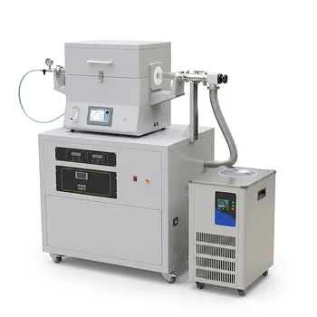
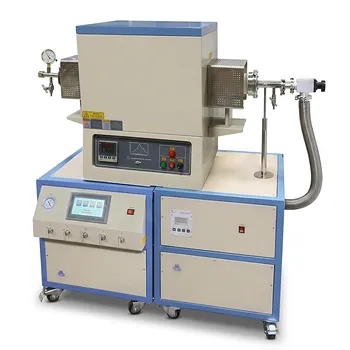
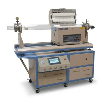
The Architecture of a CVD Machine
To achieve these capabilities, a standard CVD system integrates five critical subsystems:
- Gas Delivery System: Manages gas cylinders, mass flow controllers, and vaporizers to ensure the correct chemical mix.
- Reaction Chamber: The "reactor" where the substrate sits and the chemical reactions occur.
- Heating System: Provides the activation energy required to break chemical bonds in the precursors.
- Vacuum and Exhaust Control: Maintains the necessary pressure and safely removes hazardous chemical by-products.
- Monitoring Instrumentation: Uses tools like pyrometers or residual gas analyzers for real-time process oversight.
Understanding Technical Trade-offs
Temperature vs. Substrate Integrity
While high temperatures often lead to better crystal quality and higher purity, they can damage the underlying substrate. This necessitates the use of more expensive PECVD systems when working with low-melting-point materials.
Throughput vs. Film Quality
APCVD offers high throughput and simpler designs but often lacks the superior film uniformity and step coverage of LPCVD. Choosing between them involves balancing the need for speed against the technical requirements of the final device.
System Complexity and Footprint
Large-scale commercial CVD systems can span over 5 meters, requiring significant infrastructure and land costs. Compact systems offer a solution for R&D environments but may lack the massive batch-processing capabilities of their industrial-scale counterparts.
Making the Right Choice for Your Goal
- If your primary focus is semiconductor device fabrication: Use LPCVD or PECVD to ensure high-quality thin films with precise doping and excellent step coverage.
- If your primary focus is synthesizing high-purity synthetic diamonds: Utilize MPCVD to minimize material contamination and achieve the necessary plasma density for single-crystal growth.
- If your primary focus is producing carbon nanotubes or graphene: Select a thermal CVD system with precise gas flow regulation for carbon-based precursors and metal catalysts.
- If your primary focus is coating porous structures or fibers: Implement Chemical Vapor Infiltration (CVI) to ensure the deposition reaches the interior surfaces of the material.
By selecting the appropriate CVD variant and optimizing its gas-phase dynamics, you can engineer materials with the exact purity, thickness, and structure required for advanced technological applications.
Summary Table:
| CVD Variant | Core Technical Advantage | Primary Application Area |
|---|---|---|
| APCVD | High-throughput, simple design | Protective coatings & basic oxides |
| LPCVD | Superior film uniformity & diffusion | Semiconductor & dielectric layers |
| PECVD | Low-temperature processing | Temperature-sensitive substrates |
| MOCVD | Precise stoichiometry control | LEDs, laser diodes & optoelectronics |
| CVI | Infiltration of porous structures | Ceramic matrix composites (Aerospace) |
| MPCVD | Electrode-free, ultra-pure plasma | High-purity synthetic diamond growth |
Elevate Your Material Research with THERMUNITS
As a leading manufacturer of high-temperature laboratory equipment, THERMUNITS provides cutting-edge thermal processing solutions tailored for material science and industrial R&D. We empower researchers and manufacturers to achieve atomic-level precision in their material synthesis and heat treatment workflows.
Our comprehensive range of advanced equipment includes:
- CVD/PECVD Systems for high-purity thin films and nanostructures.
- Muffle, Vacuum, Atmosphere, and Tube Furnaces for precise heat treatment.
- Rotary, Hot Press, and Dental Furnaces designed for specialized applications.
- Electric Rotary Kilns and Vacuum Induction Melting (VIM) Furnaces for industrial-scale processing.
- Thermal Elements and a variety of laboratory heat treatment accessories.
Ready to enhance your lab's capabilities with industry-leading precision? Our technical experts are here to help you select the perfect system for your specific research goals.
Contact THERMUNITS Today for a Custom Solution
Mentioned Products
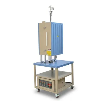
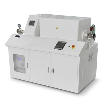
- Radio Frequency Plasma Enhanced Chemical Vapor Deposition RF PECVD System for Laboratory and Industrial Thin Film Growth
- Versatile Chemical Vapor Deposition Tube Furnace System for Advanced Material Research and Industrial Coating Processes
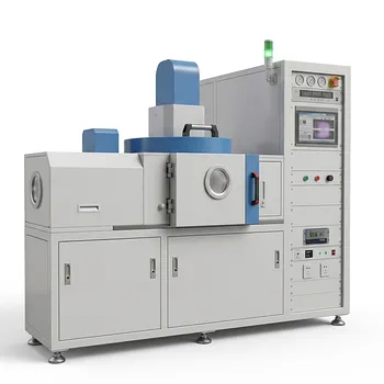
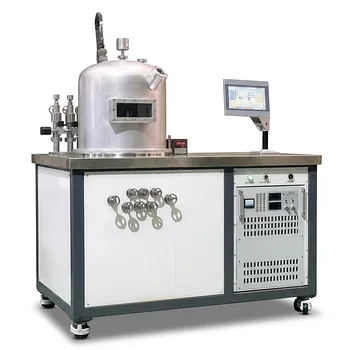
- Cylindrical Resonator MPCVD Machine System for Microwave Plasma Chemical Vapor Deposition and Lab Diamond Growth
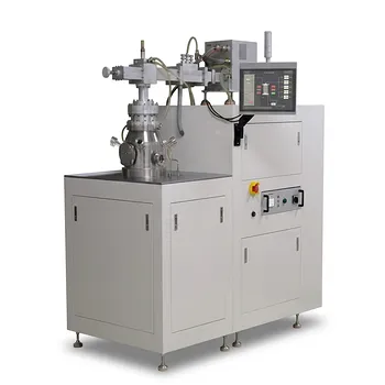
- Chemical Vapor Deposition CVD System Slide PECVD Tube Furnace with Liquid Gasifier PECVD Machine
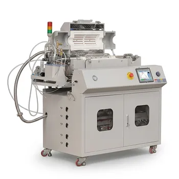
- HFCVD Machine System for Nano Diamond Coating on Drawing Dies and Industrial Tools
People Also Ask
- What role do by-product desorption and evacuation play in CVD film quality? Key Factors for High-Purity Films
- How does PECVD differ from conventional thermal CVD? Key Advantages of Low-Temperature Deposition for R&D
- What are the typical operating steps in a standard PECVD deposition cycle? Master Thin Film Process Optimization
- How does a Chemical Vapor Deposition (CVD) system ensure product quality? Precision Control for 2D Nanomaterial Growth
- What technical advantages does a CVD system offer for intermetallics? Achieve Atomic-Level Precision & Phase Purity
Tech Team · ThermUnits
Last updated on Apr 14, 2026
Related Products
Radio Frequency Plasma Enhanced Chemical Vapor Deposition RF PECVD System for Laboratory and Industrial Thin Film Growth
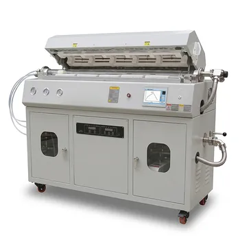
Versatile Chemical Vapor Deposition Tube Furnace System for Advanced Material Research and Industrial Coating Processes
Cylindrical Resonator MPCVD Machine System for Microwave Plasma Chemical Vapor Deposition and Lab Diamond Growth
Chemical Vapor Deposition CVD System Slide PECVD Tube Furnace with Liquid Gasifier PECVD Machine
HFCVD Machine System for Nano Diamond Coating on Drawing Dies and Industrial Tools
915MHz MPCVD Diamond Machine Microwave Plasma Chemical Vapor Deposition System Reactor
Multi Heating Zones CVD Tube Furnace System for Precision Chemical Vapor Deposition and Advanced Material Synthesis
Inclined Rotary Plasma Enhanced Chemical Vapor Deposition PECVD System for Thin Film Deposition and Nanomaterial Synthesis
Split Chamber CVD Tube Furnace with Vacuum Station Chemical Vapor Deposition System Machine
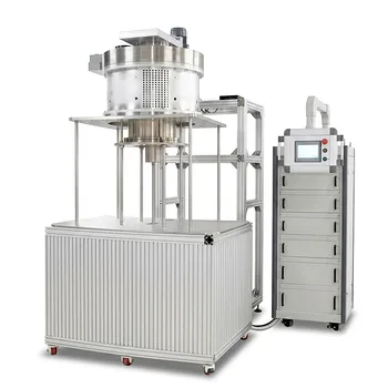
Two Zone Rotary CVD Furnace with Automatic Feeding and Receiving System for Powder Processing
Vertical Openable Tube Furnace 0-1700c High Temperature Laboratory System for CVD and Vacuum Heat Treatment
High Temperature 1700C Tube Furnace with High Vacuum Turbomolecular Pump System and Multi Channel Mass Flow Controller Gas Mixer
Dual Tube 100mm 80mm CVD Sliding Furnace with 4 Channel Gas Mixing and Vacuum System
1200°C High Temperature 4 Inch Tube Furnace with Sliding Flange for CVD Systems
1200C Max Compact Auto-Sliding PECVD Furnace with 2 Inch Tube and Vacuum Pump
5 Inch Rotary Tube Furnace with Automatic Feeding and Receiving System 1200C Three Zone CVD Powder Processing
1500C 3-Zone Rotary Tube Furnace 60mm with Automatic Powder Feeding and Receiving System for Continuous Material Synthesis
5 Inch Three Zone Rotary Tube Furnace with Integrated Gas Delivery System and 1200C Capability for Advanced Material CVD Processing
Three Temperature Zone High Temperature Vacuum Tube Furnace for CVD and Material Sintering