What are the key electronic characteristics of MPCVD diamond for power device applications? High-Voltage Efficiency
Updated 3 months ago
The electronic characteristics of Microwave Plasma Chemical Vapor Deposition (MPCVD) diamond revolve around its extreme wide-bandgap nature. Specifically, MPCVD diamond is defined by a wide bandgap of approximately 5.5 eV and an exceptionally high breakdown field strength. These properties allow for the creation of power devices—such as MOSFETs and Schottky diodes—that operate at voltages, temperatures, and frequencies far exceeding the capabilities of traditional silicon or silicon carbide.
MPCVD diamond is the ultimate semiconductor for high-power applications because its physical properties allow for efficient energy conversion under extreme conditions. By utilizing its high breakdown field and thermal stability, engineers can design smaller, more resilient components for next-generation power grids and RF systems.
The Fundamental Physics of MPCVD Diamond
The 5.5 eV Wide Bandgap
The most defining characteristic of MPCVD diamond is its wide bandgap of roughly 5.5 eV, which is significantly larger than that of Silicon (1.1 eV) or Silicon Carbide (3.2 eV).
This large energy gap means it requires much more energy to move an electron from the valence band to the conduction band. Consequently, diamond devices experience extremely low leakage currents and remain operational at temperatures where other semiconductors would suffer from thermal runaway.
Superior Breakdown Field Strength
MPCVD diamond possesses a high breakdown field, which allows the material to withstand massive electric fields without the crystal structure failing.
In practical terms, this allows for the design of devices with much thinner drift layers for a given voltage rating. This reduction in thickness minimizes on-state resistance, leading to significantly higher efficiency in power conversion.
Operational Advantages in Power Electronics
High-Voltage and High-Frequency Capability
Because diamond can handle higher electric fields, it is an ideal candidate for high-voltage power electronics.
The material's properties also support high-frequency switching, which is critical for reducing the size of passive components like inductors and capacitors. This leads to the development of power converters that are both more powerful and more compact.
Resilience to Extreme Temperatures
Diamond's intrinsic stability allows devices like MOSFETs and Schottky diodes to function in environments that would destroy standard components.
This heat tolerance reduces the need for heavy, complex cooling systems in power modules. For aerospace or automotive applications, this translates directly into weight savings and increased system reliability.
Understanding the Trade-offs
Material Growth and Consistency
While MPCVD is a preferred method for creating high-quality diamond, the process is technically demanding and slower than traditional silicon ingot pulling.
Ensuring uniform electronic properties across a large wafer remains a challenge for the industry. This can lead to variations in device performance if the growth process is not precisely controlled.
Doping and Electrical Contact Challenges
Introducing impurities to create p-type or n-type layers—a process known as doping—is more difficult in diamond than in silicon.
Achieving low-resistance ohmic contacts is also a complex engineering task due to the material's chemical inertness. These factors can currently limit the ease of mass-producing complex diamond-based integrated circuits.
How to Apply Diamond Technology to Your Project
Strategic implementation of MPCVD diamond depends on the specific demands of your power system architecture.
- If your primary focus is extreme voltage regulation: Utilize diamond Schottky diodes to take advantage of the high breakdown field and minimize switching losses.
- If your primary focus is high-temperature environments: Focus on diamond MOSFETs to eliminate the need for active cooling and simplify your thermal management design.
- If your primary focus is system miniaturization: Leverage the high-frequency capabilities of diamond to reduce the footprint of your power conversion modules.
By understanding these electronic boundaries, you can transition from traditional silicon to diamond-based architectures to unlock unprecedented levels of power density.
Summary Table:
| Electronic Characteristic | Value / Property | Power Device Advantage |
|---|---|---|
| Bandgap | ~5.5 eV (Ultrawide) | Extremely low leakage currents; high-temperature operation. |
| Breakdown Field | Exceptionally High | Thinner drift layers; lower on-state resistance and higher efficiency. |
| Thermal Stability | High Heat Tolerance | Operation in extreme environments; reduces need for complex cooling. |
| Switching Speed | High Frequency | Enables smaller passive components (inductors/capacitors). |
| Carrier Mobility | High Velocity | Supports high-power and high-frequency RF applications. |
Unlock the Potential of Next-Generation Semiconductors with THERMUNITS
Are you pushing the boundaries of material science or developing advanced power electronics? THERMUNITS is a leading manufacturer of high-temperature laboratory equipment specifically designed for industrial R&D and precision material growth.
We provide state-of-the-art CVD/PECVD systems tailored for high-quality diamond synthesis, along with a comprehensive range of thermal processing solutions including Muffle, Vacuum, Tube, and Rotary furnaces, as well as Vacuum Induction Melting (VIM) equipment. Our systems deliver the precise temperature control and atmospheric stability essential for mastering wide-bandgap material characteristics.
Ready to elevate your research and production efficiency?
Contact our expert team today to discover how THERMUNITS can provide the specialized heat treatment equipment your project demands.
Mentioned Products
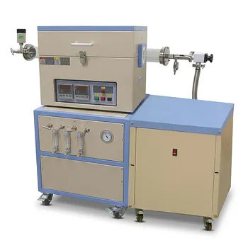
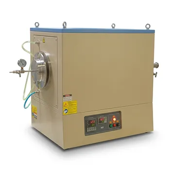
- 915MHz MPCVD Diamond Machine Microwave Plasma Chemical Vapor Deposition System Reactor
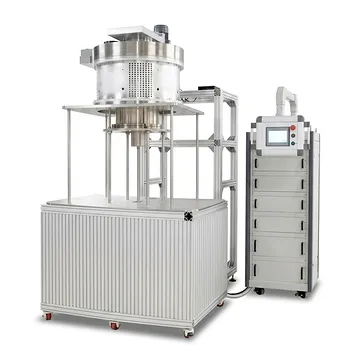
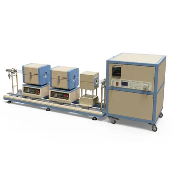
- Cylindrical Resonator MPCVD Machine System for Microwave Plasma Chemical Vapor Deposition and Lab Diamond Growth
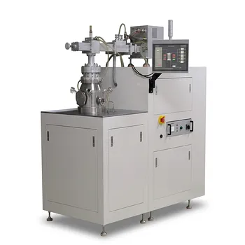
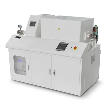
- HFCVD Machine System for Nano Diamond Coating on Drawing Dies and Industrial Tools
- 1100°C Large Diameter Quartz Tube Furnace with 24 Inch Heating Zone and Water Cooled Flanges
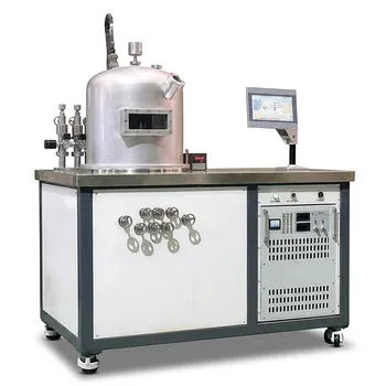
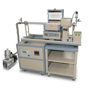
- Chemical Vapor Deposition CVD System Slide PECVD Tube Furnace with Liquid Gasifier PECVD Machine
People Also Ask
- What are the physical characteristics of the plasma generated in an MPCVD reactor? Expert Guide to CVD Plasma States
- Why are MPCVD diamond films preferred for high-energy optical components and laser windows? Unmatched Thermal Performance
- What technical parameters are critical for optimizing the growth of single-crystal diamonds in MPCVD systems? Expert Guide
- What is the fundamental working principle of a Microwave Plasma Chemical Vapor Deposition (MPCVD) machine? Expert Guide
- What thermal properties make MPCVD diamond films ideal for semiconductor thermal management? Peak 2000 W/m·K Cooling
Tech Team · ThermUnits
Last updated on Apr 14, 2026
Related Products
915MHz MPCVD Diamond Machine Microwave Plasma Chemical Vapor Deposition System Reactor
Cylindrical Resonator MPCVD Machine System for Microwave Plasma Chemical Vapor Deposition and Lab Diamond Growth
HFCVD Machine System for Nano Diamond Coating on Drawing Dies and Industrial Tools
1100°C Large Diameter Quartz Tube Furnace with 24 Inch Heating Zone and Water Cooled Flanges
Chemical Vapor Deposition CVD System Slide PECVD Tube Furnace with Liquid Gasifier PECVD Machine
1200C Max Compact Auto-Sliding PECVD Furnace with 2 Inch Tube and Vacuum Pump
1200C Dual Sliding Tube Furnace with Dual Tubes and Flanges for PECVD Processes