What thermal properties make MPCVD diamond films ideal for semiconductor thermal management? Peak 2000 W/m·K Cooling
Updated 3 months ago
MPCVD diamond films represent a paradigm shift in cooling technology due to their unmatched thermal conductivity of approximately 2000 W/m·K. This value is nearly five times higher than that of copper, allowing for the rapid removal of heat from high-power-density components. By integrating these films as heat spreaders, engineers can effectively eliminate thermal throttling in demanding applications like 5G infrastructure and data center processors.
Diamond grown via Microwave Plasma Chemical Vapor Deposition (MPCVD) provides the highest known thermal conductivity of any bulk material, enabling it to act as an "ultrasink" that manages extreme heat loads while maintaining electrical isolation.
The Science of Extreme Thermal Conductivity
Unmatched Rate of Heat Transfer
At the heart of MPCVD diamond’s appeal is its thermal conductivity of 2000 W/m·K. This allows heat to move through the material with minimal resistance, preventing the formation of localized "hotspots" that can degrade semiconductor performance.
Prevention of Thermal Throttling
Modern electronics often reduce their clock speeds to prevent overheating, a process known as thermal throttling. MPCVD diamond films dissipate heat so efficiently that devices can operate at peak performance for longer durations without reaching critical temperature thresholds.
Support for High-Power Density
As 5G/6G and AI-driven data centers squeeze more power into smaller chips, traditional materials like silicon or aluminum fail to manage the resulting heat flux. MPCVD diamond is specifically engineered to handle these high-power-density environments where conventional cooling fails.
Dual Thermal and Electrical Functionality
Electrical Insulation as a Thermal Advantage
Unlike metals, which are thermally conductive but electrically conductive, diamond is a natural electrical insulator. This allows the film to be placed in direct contact with active electronic circuits without causing short circuits, maximizing thermal extraction.
Tunable Semiconducting Properties
Through specific doping techniques during the MPCVD process, these films can be modified to exhibit semiconducting properties. This versatility means diamond can serve as both the active semiconductor material and the cooling substrate simultaneously.
Long-Term Material Stability
Diamond is chemically inert and mechanically robust, ensuring that its thermal properties do not degrade over time. This reliability is critical for infrastructure like 5G base stations, which must operate in harsh outdoor environments for decades.
Understanding the Trade-offs
The Challenge of Thermal Expansion (CTE)
One primary hurdle is the Coefficient of Thermal Expansion (CTE) mismatch between diamond and common semiconductor materials like Silicon or Gallium Nitride. If not managed during the bonding process, this difference can lead to mechanical stress or delamination as the device heats and cools.
High Cost and Manufacturing Complexity
Producing high-quality MPCVD diamond is a resource-intensive process requiring specialized microwave plasma reactors. While the performance is unrivaled, the initial cost remains significantly higher than traditional copper or ceramic heat spreaders.
Integration and Surface Roughness
As-grown MPCVD diamond films often have a crystalline surface roughness that can impede thermal contact. Achieving the necessary "atomic-level" smoothness for efficient heat transfer requires expensive post-growth polishing and processing.
Making the Right Choice for Your Goal
If your primary focus is 5G/6G Infrastructure: Utilize MPCVD diamond as a heat spreader to maintain signal integrity and prevent hardware failure in high-frequency power amplifiers.
If your primary focus is Data Center Efficiency: Implement diamond thin films to reduce the energy consumed by active cooling systems, allowing for higher rack densities and lower operational costs.
If your primary focus is Power Electronics: Leverage doped MPCVD diamond to create next-generation wide-bandgap devices that operate at higher voltages and temperatures than silicon.
By leveraging the extraordinary thermal transport of MPCVD diamond, engineers can finally overcome the thermal barriers that currently limit the next generation of high-performance computing.
Summary Table:
| Property | Metric / Characteristic | Benefit for Semiconductors |
|---|---|---|
| Thermal Conductivity | ~2000 W/m·K | 5x higher than copper; eliminates hotspots. |
| Electrical State | Natural Insulator | Allows direct contact with circuits without shorting. |
| Thermal Throttling | High Prevention | Maintains peak performance during extreme heat loads. |
| Chemical Stability | Inert & Robust | Long-term reliability for 5G and harsh environments. |
| Versatility | Tunable Doping | Can act as both cooling substrate and active semiconductor. |
Elevate Your Material R&D with THERMUNITS
As a leading manufacturer of high-temperature laboratory equipment, THERMUNITS provides the specialized tools essential for advanced material science and industrial R&D. Our comprehensive range of thermal processing solutions—including high-precision CVD/PECVD systems, Vacuum and Atmosphere furnaces, and Muffle furnaces—is designed to help you achieve the exact conditions required for high-performance MPCVD diamond growth and semiconductor testing.
Whether you are developing next-generation 5G infrastructure or high-power-density AI processors, our expert team is ready to provide the heat treatment equipment you need to succeed.
Ready to optimize your thermal management research?
Contact our specialists today for a tailored solution!
Mentioned Products
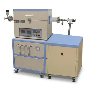
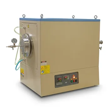
- 915MHz MPCVD Diamond Machine Microwave Plasma Chemical Vapor Deposition System Reactor
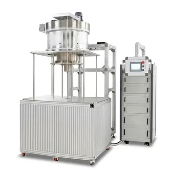
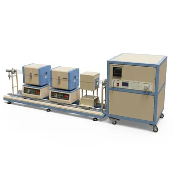
- Cylindrical Resonator MPCVD Machine System for Microwave Plasma Chemical Vapor Deposition and Lab Diamond Growth
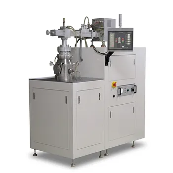
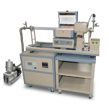
- HFCVD Machine System for Nano Diamond Coating on Drawing Dies and Industrial Tools
- 1100°C Large Diameter Quartz Tube Furnace with 24 Inch Heating Zone and Water Cooled Flanges
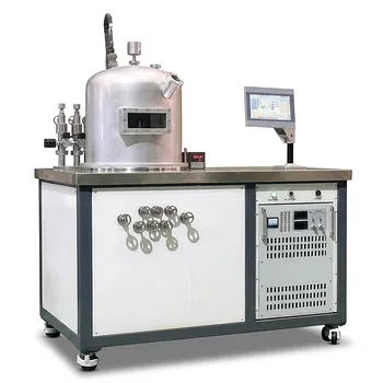
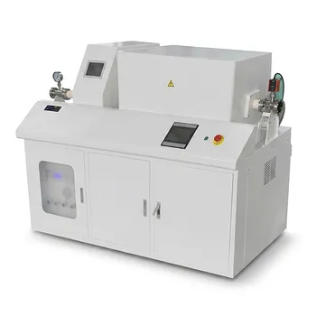
- Chemical Vapor Deposition CVD System Slide PECVD Tube Furnace with Liquid Gasifier PECVD Machine
People Also Ask
- What is the significance of substrate capacity and scalability in modern MPCVD reactor designs? Scale Your Production
- What are the physical characteristics of the plasma generated in an MPCVD reactor? Expert Guide to CVD Plasma States
- What are the key electronic characteristics of MPCVD diamond for power device applications? High-Voltage Efficiency
- What is the fundamental working principle of a Microwave Plasma Chemical Vapor Deposition (MPCVD) machine? Expert Guide
- What are the typical operating pressure ranges and vacuum requirements for MPCVD systems? Optimize Your Material Growth
Tech Team · ThermUnits
Last updated on Apr 14, 2026
Related Products
915MHz MPCVD Diamond Machine Microwave Plasma Chemical Vapor Deposition System Reactor
Cylindrical Resonator MPCVD Machine System for Microwave Plasma Chemical Vapor Deposition and Lab Diamond Growth
HFCVD Machine System for Nano Diamond Coating on Drawing Dies and Industrial Tools
1100°C Large Diameter Quartz Tube Furnace with 24 Inch Heating Zone and Water Cooled Flanges
Chemical Vapor Deposition CVD System Slide PECVD Tube Furnace with Liquid Gasifier PECVD Machine
1200C Max Compact Auto-Sliding PECVD Furnace with 2 Inch Tube and Vacuum Pump
1200C Dual Sliding Tube Furnace with Dual Tubes and Flanges for PECVD Processes