The Geometry of Silence: Why Depth Demands a Chemical Solution
Jul 17, 2026
The Invisible Wall of the Sub-10nm Node
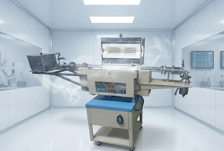
In the world of semiconductor fabrication, we are constantly fighting against the physics of scale.
As features shrink, they don't just get smaller; they get deeper. We call this the high-aspect-ratio (HAR) challenge. Imagine trying to paint the very bottom of a well that is a mile deep but only a few feet wide.
If you use a spray gun (Physical Vapor Deposition), the paint hits the top edges and dries before it ever reaches the bottom. This is the "shadowing effect," and in a microprocessor, it leads to catastrophic failure.
To solve this, we don't change the tool; we change the state of matter. We move from the physical to the chemical.
The Tyranny of the Line-of-Sight
Physical Vapor Deposition (PVD) is an honest, mechanical process. It moves atoms from Point A to Point B in a straight line.
But honesty has its limits. In modern 3D architectures—like FinFETs or 3D NAND—the path to the surface is rarely a straight line.
- The Shadowing Problem: Atoms in a PVD stream behave like light. Where they cannot "see," they cannot coat.
- The Keyhole Risk: Material builds up at the "neck" of a trench, sealing it off before the center is filled.
- The Structural Void: These trapped air pockets (voids) act as ticking time bombs for electrical failure.
The Logic of Conformality
Chemical Vapor Deposition (CVD) operates on a different psychological principle: ubiquity.
Instead of a directional spray, CVD uses a gas-phase precursor. The gas doesn't care about "line-of-sight." It fills the entire chamber, permeating every microscopic crevice like a fog in a valley.
The film grows not because an atom was "thrown" there, but because a chemical reaction was triggered there.
Why CVD Wins the Depth War
- Surface-Controlled Growth: Because the reaction happens on the heated surface itself, the growth is uniform across all 3D geometries.
- 95% Step Coverage: While PVD struggles to maintain thickness on vertical sidewalls, CVD achieves nearly perfect conformality.
- Void-Free Filling: By regulating the flow and pressure, engineers can ensure that the bottom of a trench fills at the same rate as the top.
The Strategic Trade-offs: Heat as Currency
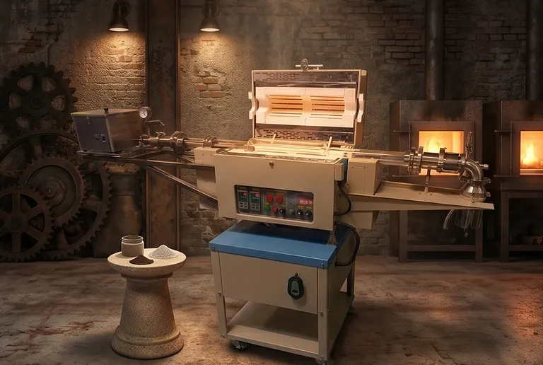
In engineering, you never get something for nothing. To buy the uniformity of CVD, you must pay in "Thermal Budget."
CVD requires specific, often high temperatures to break chemical bonds and initiate deposition. This creates a psychological tension for the researcher: how do you achieve perfect film quality without melting the layers you’ve already built?
Balancing the Budget
| Feature | CVD (The Chemical Path) | PVD (The Physical Path) |
|---|---|---|
| Mechanism | Surface Reaction | Ballistic Transfer |
| Coverage | Superior (Conformal) | Limited (Directional) |
| Complexity | High (Precursors & Byproducts) | Low (Solid Targets) |
| Temperature | Usually Higher | Usually Lower |
| Best Use Case | Deep Trenches & Complex Vias | Flat Surfaces & Interconnects |
The Engineer’s Romanticism: Precision in Chaos
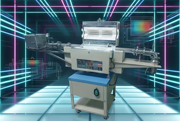
There is a certain beauty in a CVD reactor. Inside a vacuum tube, amidst controlled heat, molecules are dancing in a calculated chaos.
By fine-tuning the gas flow ratios and the thermal field, we aren't just "coating" a surface; we are orchestrating the assembly of matter at the atomic level. This is how we achieve the precise stoichiometry required for MXenes, graphene, and advanced epitaxial layers.
Engineering the Future of Thermal Processing
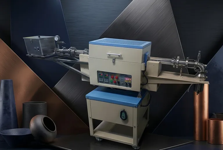
Achieving this level of precision requires more than just chemistry; it requires a perfectly controlled environment. At THERMUNITS, we understand that the difference between a breakthrough and a failure lies in the stability of the thermal field.
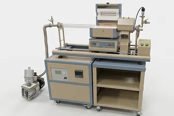
We provide the "high-temperature cathedrals" where these reactions take place. From CVD/PECVD systems to high-vacuum induction melting furnaces, our equipment is designed for the rigorous demands of modern R&D.
Whether you are scaling sub-10nm nodes or pioneering new 2D materials, the equipment must be as precise as the science.
Quick Links
Suggested Products
Chemical Vapor Deposition CVD System Slide PECVD Tube Furnace with Liquid Gasifier PECVD Machine Versatile Chemical Vapor Deposition Tube Furnace System for Advanced Material Research and Industrial Coating Processes Radio Frequency Plasma Enhanced Chemical Vapor Deposition RF PECVD System for Laboratory and Industrial Thin Film Growth 915MHz MPCVD Diamond Machine Microwave Plasma Chemical Vapor Deposition System Reactor Inclined Rotary Plasma Enhanced Chemical Vapor Deposition PECVD System for Thin Film Deposition and Nanomaterial SynthesisFurther Reading
The Choreography of Carbon: Why CVD Precision Defines the Next Era of Material Science The Architecture of Ions: Decoding the Geometry of Plasma Coupling The Architecture of Clouds: Mastering the RF Equilibrium in PECVD The Low-Temperature Alchemy: Navigating the Thermal Budget with PECVD The Alchemy of Cold Fire: Decoupling Energy from Temperature in Thin Film Deposition
ThermUnits
Last updated on Apr 14, 2026
Related Products
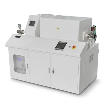
Chemical Vapor Deposition CVD System Slide PECVD Tube Furnace with Liquid Gasifier PECVD Machine
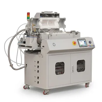
Versatile Chemical Vapor Deposition Tube Furnace System for Advanced Material Research and Industrial Coating Processes
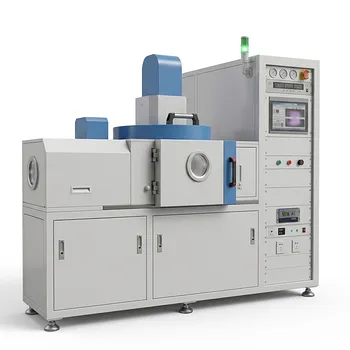
Radio Frequency Plasma Enhanced Chemical Vapor Deposition RF PECVD System for Laboratory and Industrial Thin Film Growth
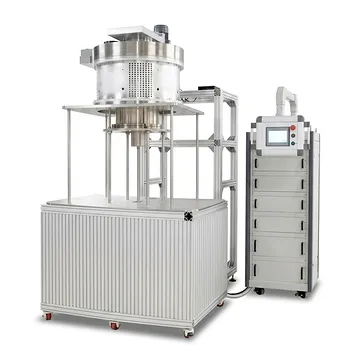
915MHz MPCVD Diamond Machine Microwave Plasma Chemical Vapor Deposition System Reactor
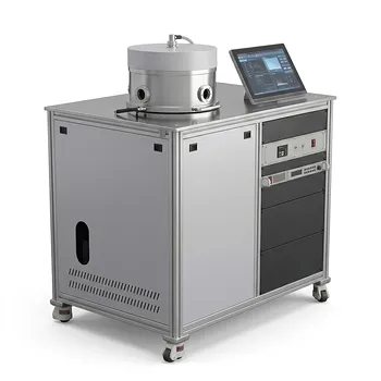
Inclined Rotary Plasma Enhanced Chemical Vapor Deposition PECVD System for Thin Film Deposition and Nanomaterial Synthesis
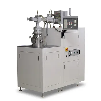
Cylindrical Resonator MPCVD Machine System for Microwave Plasma Chemical Vapor Deposition and Lab Diamond Growth
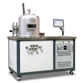
HFCVD Machine System for Nano Diamond Coating on Drawing Dies and Industrial Tools
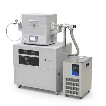
Split Chamber CVD Tube Furnace with Vacuum Station Chemical Vapor Deposition System Machine
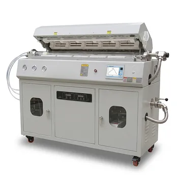
Multi Heating Zones CVD Tube Furnace System for Precision Chemical Vapor Deposition and Advanced Material Synthesis
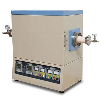
High Temperature 1700C Dual Zone Tube Furnace for Material Science and Industrial Chemical Vapor Deposition Research
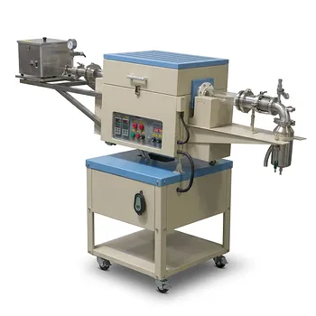
Two Zone Rotary CVD Furnace with Automatic Feeding and Receiving System for Powder Processing