The Low-Temperature Alchemy: Navigating the Thermal Budget with PECVD
Jul 24, 2026
The Tyranny of the Thermal Budget
In the world of semiconductor fabrication, heat is both a creator and a destroyer. To grow a crystal, you need energy; to bond a film, you need heat. But as devices shrink to the nanometer scale, the "thermal budget"—the total amount of heat a wafer can withstand before its delicate structures degrade—becomes a zero-sum game.
If you exceed this budget, dopants migrate where they shouldn't, and metal interconnects, like copper or aluminum, begin to soften or melt. This is the central tension of modern engineering: How do you build a skyscraper of atoms without burning the foundation?
Plasma-Enhanced Chemical Vapor Deposition (PECVD) is the industry’s elegant answer to this paradox. By using a plasma to provide the activation energy for chemical reactions, we can deposit high-quality thin films at temperatures that keep the underlying circuitry safe.
The Invisible Architecture: ILD and IMD
The most common application of PECVD is the creation of the "insulation" within the chip. Interlayer Dielectrics (ILD) and Inter-metal Dielectrics (IMD) are the silent guardians of electrical integrity.
Without these layers, the dense web of wiring inside a processor would short-circuit instantly. Because PECVD operates at low temperatures (often below 400°C), it can lay down these insulating blankets directly over metal lines without causing thermal stress or structural failure.
- Low-k Dielectrics: Reducing capacitance to speed up signal transmission.
- Uniformity: Ensuring that every wire, no matter how deep in the stack, is perfectly isolated.
The Shield: Passivation and Etch-Stops
A chip is a fragile thing. Left exposed, moisture and contaminants from the environment would corrode it within days. PECVD is used to grow the "passivation layer"—the final, tough skin of the semiconductor.
Usually composed of Silicon Nitride (SiNx), this layer is nearly impermeable. Furthermore, PECVD creates the "etch-stop" layers—precise chemical markers that tell a plasma etch or a polishing tool exactly where to stop. In a world of 3D transistors, a nanometer too deep is the difference between a flagship processor and a piece of scrap silicon.
Scaling Up: 3D Packaging and Beyond
As Moore’s Law encounters physical limits, the industry has turned to "Heterogeneous Integration"—stacking chips like LEGO bricks. This is where PECVD proves its versatility in 2.5D and 3D packaging.
| Application | Primary Function | Key Materials |
|---|---|---|
| TSV Passivation | Insulating vertical electrical connections | High-conformality films |
| Hybrid Bonding | Enabling dense chip-to-chip stacking | Dielectric insulators |
| MEMS/Sensors | Creating structural and sacrificial layers | Amorphous Silicon (a-Si) |
| Gate Dielectrics | Transistor isolation and gate definition | Silicon Dioxide/Nitride |
The Engineer’s Trade-off: Purity vs. Protection
Every engineering victory comes with a price. In the case of PECVD, the trade-off is often chemical purity. Because the process happens at lower temperatures, hydrogen or other precursors can sometimes remain trapped in the film.
Furthermore, the plasma itself—a chaotic soup of ions—can cause "plasma-induced damage" if not controlled with surgical precision. The modern engineer doesn't just "run a process"; they balance RF power, frequency, and gas flow to find the "Goldilocks zone" where the film is dense, the stress is low, and the substrate remains unharmed.
Systemic Precision with THERMUNITS
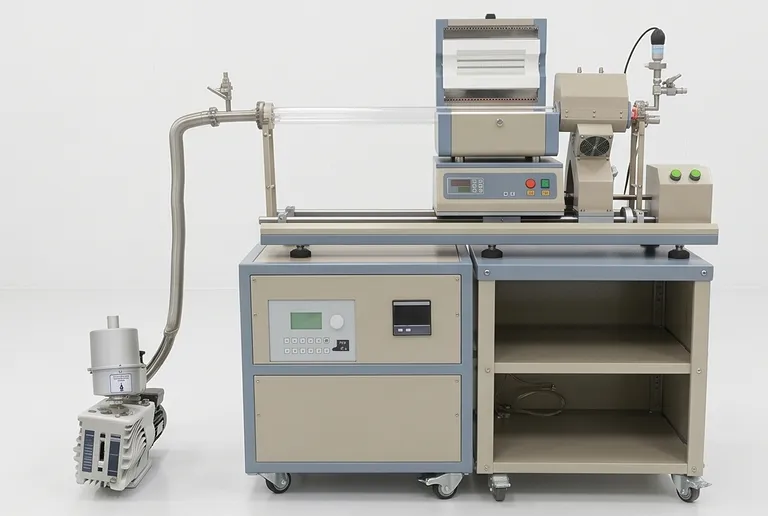
Moving from a theoretical design to a functional thin film requires more than just a recipe; it requires a controlled environment where variables are eliminated. At THERMUNITS, we understand that in R&D and high-tech manufacturing, the furnace is the heart of the laboratory.
We specialize in high-temperature thermal processing solutions designed to meet the rigorous demands of material science. Our systems are built for engineers who refuse to compromise on precision:
- Precision PECVD & CVD Systems: Engineered for controlled thin-film growth and high-aspect-ratio conformality.
- Comprehensive Thermal Range: From Muffle and Vacuum furnaces to specialized Vacuum Induction Melting (VIM).
- Advanced Materials Focus: Supporting the development of next-gen logic, memory, and 3D packaging.
The future of semiconductor technology isn't just about smaller transistors; it's about smarter thermal management. Whether you are developing amorphous silicon for TFTs or insulating Through-Silicon Vias for AI hardware, the right equipment is your most critical precursor.
To explore how our thermal processing solutions can refine your R&D workflow, Contact Our Experts.
Quick Links
Suggested Products
Inclined Rotary Plasma Enhanced Chemical Vapor Deposition PECVD System for Thin Film Deposition and Nanomaterial Synthesis Radio Frequency Plasma Enhanced Chemical Vapor Deposition RF PECVD System for Laboratory and Industrial Thin Film Growth Chemical Vapor Deposition CVD System Slide PECVD Tube Furnace with Liquid Gasifier PECVD Machine 1200C Max Compact Auto-Sliding PECVD Furnace with 2 Inch Tube and Vacuum Pump 1200C Dual Sliding Tube Furnace with Dual Tubes and Flanges for PECVD ProcessesFurther Reading
The Alchemy of Cold Fire: Decoupling Energy from Temperature in Thin Film Deposition The Architecture of Ions: Decoding the Geometry of Plasma Coupling The Architecture of Clouds: Mastering the RF Equilibrium in PECVD The Geometry of Silence: Why Depth Demands a Chemical Solution The Choreography of Carbon: Why CVD Precision Defines the Next Era of Material Science
ThermUnits
Last updated on Apr 14, 2026
Related Products
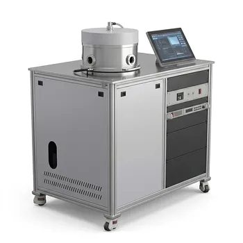
Inclined Rotary Plasma Enhanced Chemical Vapor Deposition PECVD System for Thin Film Deposition and Nanomaterial Synthesis
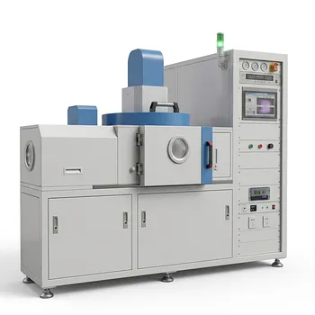
Radio Frequency Plasma Enhanced Chemical Vapor Deposition RF PECVD System for Laboratory and Industrial Thin Film Growth
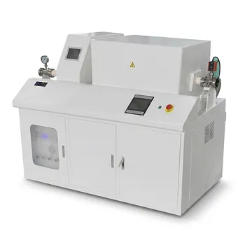
Chemical Vapor Deposition CVD System Slide PECVD Tube Furnace with Liquid Gasifier PECVD Machine
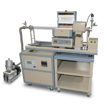
1200C Max Compact Auto-Sliding PECVD Furnace with 2 Inch Tube and Vacuum Pump
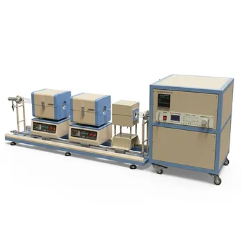
1200C Dual Sliding Tube Furnace with Dual Tubes and Flanges for PECVD Processes
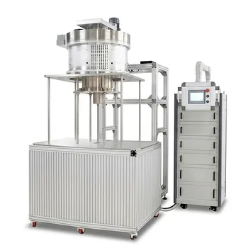
915MHz MPCVD Diamond Machine Microwave Plasma Chemical Vapor Deposition System Reactor
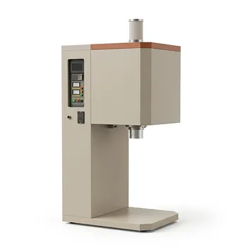
Vertical Openable Tube Furnace 0-1700c High Temperature Laboratory System for CVD and Vacuum Heat Treatment
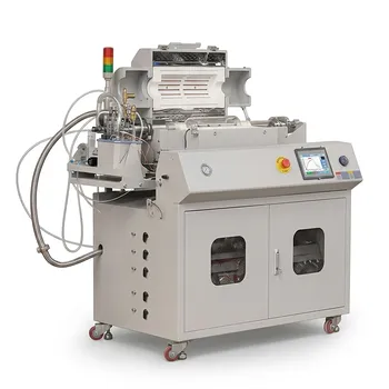
Versatile Chemical Vapor Deposition Tube Furnace System for Advanced Material Research and Industrial Coating Processes
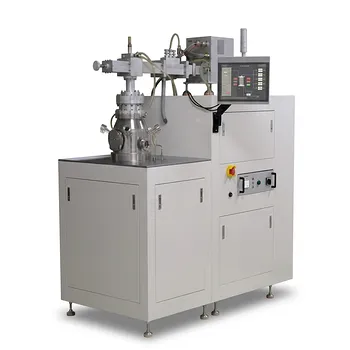
Cylindrical Resonator MPCVD Machine System for Microwave Plasma Chemical Vapor Deposition and Lab Diamond Growth
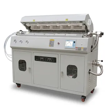
Multi Heating Zones CVD Tube Furnace System for Precision Chemical Vapor Deposition and Advanced Material Synthesis
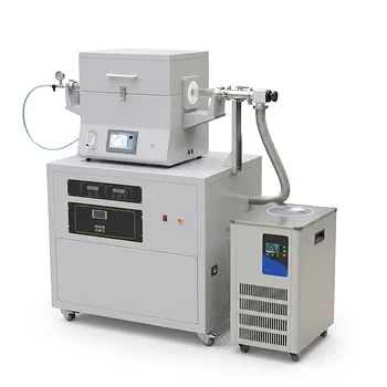
Split Chamber CVD Tube Furnace with Vacuum Station Chemical Vapor Deposition System Machine
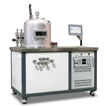
HFCVD Machine System for Nano Diamond Coating on Drawing Dies and Industrial Tools
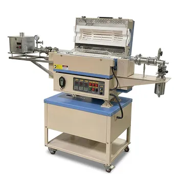
5 Inch Rotary Tube Furnace with Automatic Feeding and Receiving System 1200C Three Zone CVD Powder Processing
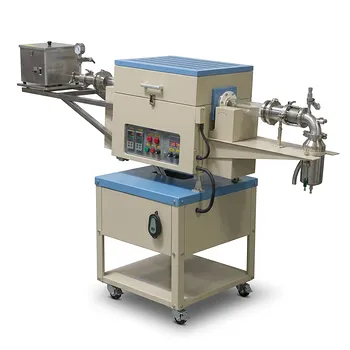
Two Zone Rotary CVD Furnace with Automatic Feeding and Receiving System for Powder Processing
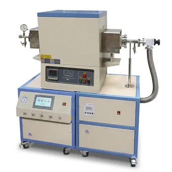
High Temperature 1700C Tube Furnace with High Vacuum Turbomolecular Pump System and Multi Channel Mass Flow Controller Gas Mixer
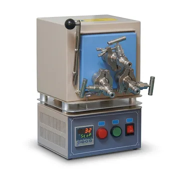
Triple Tube Compact Hybrid Muffle Furnace 1000C High Vacuum Thermal Processing System
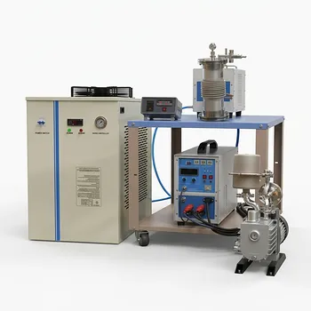
Induction Heating System with Temperature Control for High Temperature Vacuum Sintering and Melting
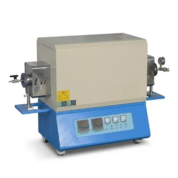
High Temperature Dual Zone Vacuum Tube Furnace for Material Research and CVD Processing
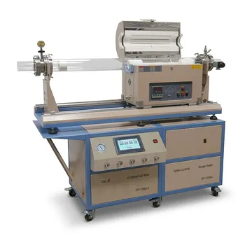
Dual Tube 100mm 80mm CVD Sliding Furnace with 4 Channel Gas Mixing and Vacuum System