The Thermal Sanctity of Flatland: Why Vacuum Annealing Defines the Limit of 2D Electronics
Jun 29, 2026
The Perfection Gap in Two Dimensions
In the world of 2D semiconductors—materials like Tungsten Disulfide (WS2) that are only atoms thick—the promise is infinite speed and zero friction. But the reality is often messy.
We design devices with mathematical precision, yet when they emerge from the lithography lab, they underperform. They lag. They resist.
This is the "perfection gap." It is caused by the invisible debris of fabrication: microscopic polymer residues, trapped water molecules, and atomic-scale scars in the crystal lattice. Vacuum annealing is the systemic solution to these invisible saboteurs.
The Ghost of Lithography: Photoresist and Moisture
Fabrication is a violent process for a material that is essentially a single layer of atoms. The chemical "masks" (photoresists) used to pattern circuits never truly leave; they leave behind a thin film of carbon-based clutter.
These residues act as scattering centers. Imagine a sprinter trying to run through a crowd; the electrons lose momentum, heat is generated, and carrier mobility plummets.
Furthermore, our atmosphere is a hostile environment. Water molecules nestle between the 2D material and the silicon substrate, creating "charge traps." These traps cause electrical hysteresis—a memory effect where the device doesn't respond consistently to voltage.
Vacuum annealing performs a "thermal cleanup":
- Sublimation: High heat under vacuum forces photoresist residues to detach and evacuate.
- Dehydration: Trapped moisture is evaporated, clearing the interface for better electronic coupling.
The Healing of the Lattice
Even the best-grown transition metal dichalcogenide (TMDC) is born with defects. Vacancies—holes where an atom should be—distort the local electric field.
Heat is the energy of motion. In a controlled vacuum environment, we provide the atoms with just enough energy to "settle" into their rightful places. We aren't just cleaning the surface; we are repairing the architecture.
Impact of Thermal Restoration
| Issue Addressed | Physical Mechanism | Resulting Performance |
|---|---|---|
| Lattice Vacancies | Atomic reorganization | Higher Carrier Mobility |
| Interface Stress | Mechanical relaxation | Stable Threshold Voltage |
| Contact Resistance | Improved electronic coupling | Efficient Charge Transfer |
The Metal-Semiconductor Paradox
The most difficult part of a 2D device is the "handshake"—the point where a 3D metal contact meets a 2D channel. Often, there is a gap, a barrier of resistance that kills efficiency.
Vacuum annealing facilitates a subtle atomic migration. It brings the metal and the semiconductor into a more intimate contact, reducing the "Schottky barrier" and allowing electrons to flow across the boundary with minimal resistance.
The Psychology of the Thermal Budget
Every material has a "thermal budget"—a finite amount of heat it can withstand before it begins to decompose. In engineering, as in life, more is not always better.
If you exceed the budget, your metal contacts might diffuse into the semiconductor, or the 2D lattice might vaporize entirely. The challenge is not just reaching a temperature; it is the precision of the ramp, the integrity of the vacuum, and the uniformity of the heat.
A poor vacuum is worse than no vacuum. If oxygen molecules remain, the high heat will cause the semiconductor to oxidize, turning a high-performance material into a useless insulator.
Engineering the Intrinsic State
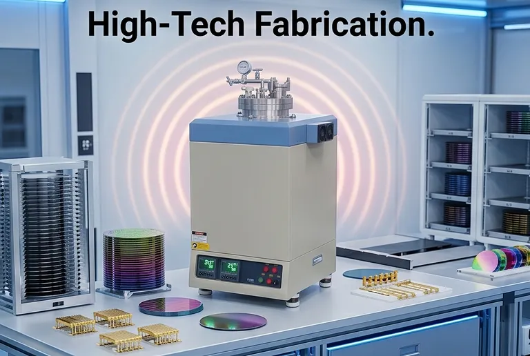
At THERMUNITS, we build the cathedrals where this atomic-scale restoration takes place. We understand that for a material scientist, a furnace is not just a heater—it is a tool for controlling entropy.
Our high-temperature laboratory solutions are engineered for the specific rigors of 2D material research and industrial R&D:
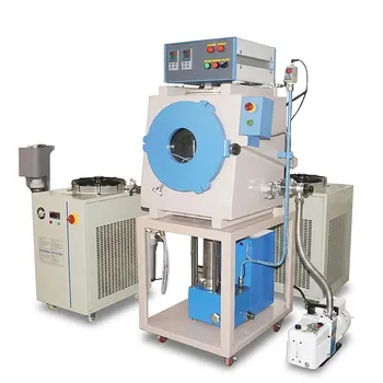
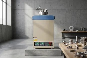
- Vacuum & Atmosphere Furnaces: Achieving the ultra-clean environments necessary to prevent oxidation during annealing.
- CVD/PECVD Systems: For the bottom-up synthesis of pristine 2D layers.
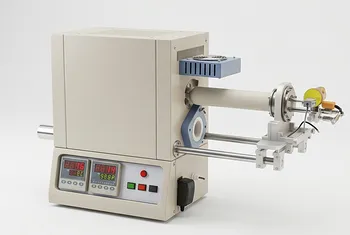
- Tube & Muffle Furnaces: Providing the thermal uniformity required to respect the delicate "thermal budget" of your devices.
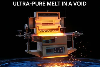
- Advanced Solutions: From Vacuum Induction Melting (VIM) to specialized Hot Press furnaces for composite materials.
By removing the extrinsic noise of fabrication, we allow the intrinsic beauty of 2D physics to shine through. Precision heat treatment is the final, essential step in moving from a laboratory curiosity to a world-changing technology.
To discuss the thermal parameters for your next breakthrough, Contact Our Experts
Quick Links
Suggested Products
High Temperature 1000C Vacuum Furnace with 8 Inch ID Chamber for Material Sintering and Research Annealing Double Temperature Zone Double Cover Tube Furnace for High Temperature CVD and Vacuum Annealing High Temperature Cold Wall Vacuum Furnace for Advanced Material Sintering and Annealing 1600C Heating Area 200x200x300mm Three Temperature Zone High Temperature Vacuum Tube Furnace for CVD and Material Sintering High Temperature Vertical Atmosphere Controlled Furnace with Automatic Bottom Loading and 1700°C Capacity for Advanced Material ResearchFurther Reading
The Architecture of Absence: Why Vacuum Technology Defines the Future of Flight The Invisible Chemistry of High Heat: Designing Certainty into Vacuum Hot-Zones The Purity of Absence: Why the Human Body Demands Vacuum-Processed Metallurgy The Silent Architect: Why the Thermal Field Dictates the Destiny of FeNi Nanostructures The Geometry of the Invisible: Why High Vacuum is the Silent Architect of La2O2S Clarity
ThermUnits
Last updated on Apr 14, 2026
Related Products
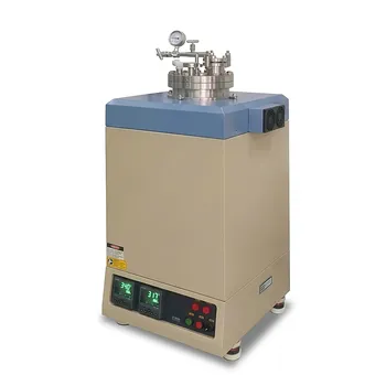
High Temperature 1000C Vacuum Furnace with 8 Inch ID Chamber for Material Sintering and Research Annealing
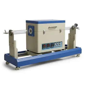
Double Temperature Zone Double Cover Tube Furnace for High Temperature CVD and Vacuum Annealing
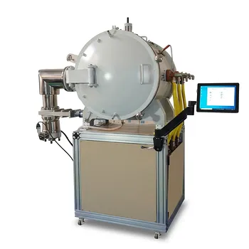
High Temperature Cold Wall Vacuum Furnace for Advanced Material Sintering and Annealing 1600C Heating Area 200x200x300mm
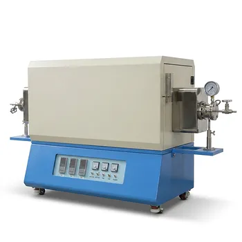
Three Temperature Zone High Temperature Vacuum Tube Furnace for CVD and Material Sintering
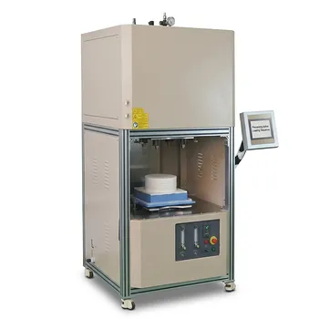
High Temperature Vertical Atmosphere Controlled Furnace with Automatic Bottom Loading and 1700°C Capacity for Advanced Material Research
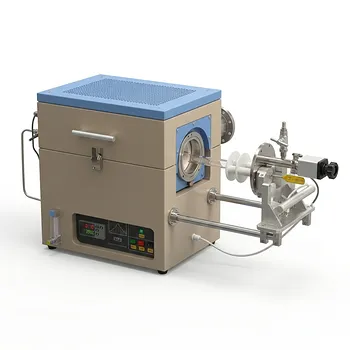
Compact Atmosphere Controlled Rapid Thermal Processing RTP Furnace with 4 Inch ID Quartz Tube 1100C
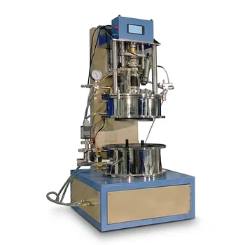
2500C High Vacuum Ultrafast Heating Pellet Press with Automated 8 Sample Loading System
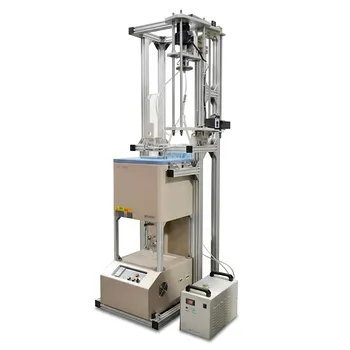
500C Vacuum Vertical Tube Furnace 84mm OD Sample Rotation Lifting System
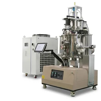
950C Rapid Thermal Processing Furnace for 12 Inch Wafer CSS Coating with Rotating Substrate Holder
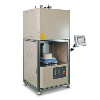
High Temperature Vertical Atmosphere Controlled Furnace 1700C Automatic Bottom Loading 13 Liter Vacuum Thermal System
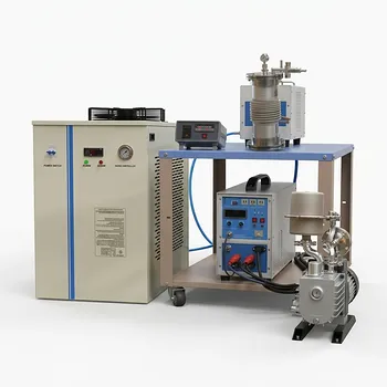
Induction Heating System with Temperature Control for High Temperature Vacuum Sintering and Melting
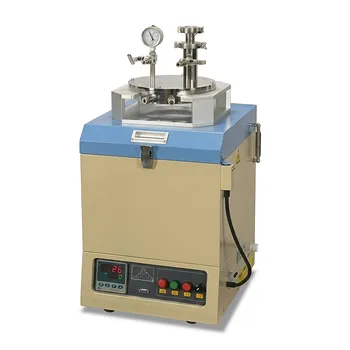
Vertical Vacuum Furnace 1100C High Temperature 8 Inch Quartz Chamber Water Cold Flange System
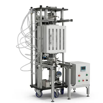
Industrial High Temperature Vacuum Hot Press Furnace and Heated Vacuum Press Machine for Material Science Sintering
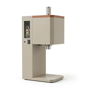
Vertical Openable Tube Furnace 0-1700c High Temperature Laboratory System for CVD and Vacuum Heat Treatment
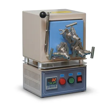
Triple Tube Compact Hybrid Muffle Furnace 1000C High Vacuum Thermal Processing System