What are the primary advantages of using an MOCVD system compared to PVD for 2D SnSe2 films? Gain Atomic Precision
Updated 3 months ago
MOCVD provides a level of atomic-scale precision that traditional PVD cannot match for 2D materials. By utilizing precise control of gas-phase precursor concentrations and a uniform flow field design, MOCVD ensures the consistent transport of materials across large areas like 2-inch sapphire substrates. This chemical approach enables more accurate layer-count control and superior in-plane uniformity, which are the fundamental requirements for achieving full coverage and high-quality SnSe2 thin films.
Core Takeaway: For wafer-scale tin selenide synthesis, MOCVD is the superior choice because it replaces the "line-of-sight" limitations of PVD with a highly controllable chemical reaction mechanism, ensuring uniform thickness and customizable microstructures across the entire substrate.
Precision Engineering of Thin Film Growth
Accurate Layer-Count Control
MOCVD operates through high-temperature chemical reactions rather than simple physical vapor transport. This allow researchers to manage the growth process at the molecular level, ensuring that the number of atomic layers is consistent across the entire wafer surface.
Superior In-Plane Uniformity
The system’s design prioritizes a uniform flow field, which prevents the uneven distribution of precursors. This results in a tin selenide film that maintains the same electrical and structural properties from the center of the wafer to its edges.
Full Substrate Coverage
Achieving a continuous, "closed" film is a significant challenge for 2D materials like SnSe2. MOCVD facilitates lateral grain growth, encouraging the film to close gaps and form a continuous layer that is essential for industrial-grade semiconductor applications.
Microstructural and Chemical Flexibility
Tailoring Grain Size and Orientation
MOCVD equipment allows for the flexible adjustment of gas ratios, reaction pressures, and deposition temperatures. This flexibility enables engineers to adjust grain sizes across a broad range (typically 20nm to 130nm) and induce specific crystal orientations to meet specific device requirements.
Precise Stoichiometric Control
By adjusting the partial pressure ratios of the precursor gases, MOCVD allows for the fine-tuning of the film's chemical stoichiometry. This is critical for 2D tin selenide, where even minor deviations in the tin-to-selenium ratio can drastically alter electronic or optical functions.
High Material Purity
Unlike liquid-phase methods, MOCVD eliminates risks associated with acid corrosion or impurity residues. The vacuum-sealed chemical environment ensures that the resulting MXenes or chalcogenides like SnSe2 have high crystallinity and fewer grain boundaries.
Understanding the Trade-offs
Thermal Stress and Substrate Sensitivity
MOCVD typically requires higher processing temperatures to trigger the necessary chemical reactions. This can lead to increased thermal mismatch and internal stress between the film and the substrate, whereas PVD’s lower-temperature process can minimize these issues.
Surface Roughness and Density
In some applications, PVD-grown films may exhibit lower surface roughness and higher density compared to chemical vapor methods. For certain piezoelectric or high-density electrode applications, the physical deposition approach may offer better inhibition of substrate decomposition.
System Complexity and Cost
MOCVD systems involve complex gas handling and toxic precursors, leading to higher maintenance costs and stricter safety protocols. While more stable for long-term thermal processing, the initial setup and operational overhead are often higher than those of a standard PVD evaporation or sputtering system.
Making the Right Choice for Your Goal
To determine the best deposition method for your tin selenide project, consider your primary performance metric:
- If your primary focus is wafer-scale continuity and layer precision: MOCVD is the definitive choice due to its superior flow field design and chemical kinetics.
- If your primary focus is minimizing thermal stress on sensitive substrates: PVD may be preferable as it allows for lower deposition temperatures that reduce internal strain.
- If your primary focus is complex 3D architecture or step coverage: MOCVD is required to ensure void-free filling and uniform thickness over non-planar structures.
- If your primary focus is maximizing film density and surface smoothness: PVD typically yields a more compact film with a lower roughness profile.
MOCVD transforms the synthesis of 2D tin selenide from a simple coating process into a precise, scalable chemical engineering solution.
Summary Table:
| Feature | MOCVD (Chemical) | PVD (Physical) |
|---|---|---|
| Control Mechanism | Chemical kinetics & gas flow | Physical line-of-sight transport |
| Layer Precision | Atomic-scale layer-count control | Approximate thickness control |
| Uniformity | Superior in-plane uniformity | Risk of center-to-edge variance |
| Growth Temp. | Higher (triggers reactions) | Lower (less thermal stress) |
| Film Density | High crystallinity, lower density | High density, low roughness |
| Complexity | High (gas handling/safety) | Moderate (vacuum-focused) |
Elevate Your Material Synthesis with THERMUNITS Precision Equipment
Are you looking to achieve atomic-scale precision and superior uniformity in your 2D material research? THERMUNITS is a leading manufacturer of high-temperature laboratory equipment specifically designed for material science and industrial R&D.
We offer a comprehensive range of thermal processing solutions tailored to your specific deposition needs, including:
- CVD/PECVD Systems for advanced chemical vapor deposition.
- Muffle, Vacuum, Atmosphere, and Tube Furnaces for precise heat treatment.
- Hot Press Furnaces & Vacuum Induction Melting (VIM) Furnaces for high-density material production.
- Rotary Kilns & Dental Furnaces for specialized industrial applications.
Whether you are scaling up tin selenide production or developing next-generation semiconductors, our equipment ensures the stoichiometric control and material purity your project demands.
Ready to optimize your lab's performance? Contact THERMUNITS Today for a Professional Consultation
References
- Sungyeon Kim, Joonki Suh. Phase‐Centric MOCVD Enabled Synthetic Approaches for Wafer‐Scale 2D Tin Selenides. DOI: 10.1002/adma.202400800
Mentioned Products
- Versatile Chemical Vapor Deposition Tube Furnace System for Advanced Material Research and Industrial Coating Processes
- Chemical Vapor Deposition CVD System Slide PECVD Tube Furnace with Liquid Gasifier PECVD Machine
- HFCVD Machine System for Nano Diamond Coating on Drawing Dies and Industrial Tools
- Multi Heating Zones CVD Tube Furnace System for Precision Chemical Vapor Deposition and Advanced Material Synthesis
- Radio Frequency Plasma Enhanced Chemical Vapor Deposition RF PECVD System for Laboratory and Industrial Thin Film Growth
People Also Ask
- How does a sliding rail design benefit the CVD process within a furnace ventilation hood? Enhance Control & Quenching
- What role do by-product desorption and evacuation play in CVD film quality? Key Factors for High-Purity Films
- How does the deposition process occur within a Chemical Vapor Deposition (CVD) reactor? Explore the 5-Stage Growth Cycle
- Why is CVD preferred over PVD for high-aspect-ratio features? Superior Conformality for Semiconductor Fabrication
- How do temperature regimes influence the growth rate of films in a CVD system? Master CVD Kinetics for Superior Thin Films

Tech Team · ThermUnits
Last updated on Jun 03, 2026
Related Products
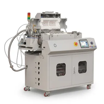
Versatile Chemical Vapor Deposition Tube Furnace System for Advanced Material Research and Industrial Coating Processes
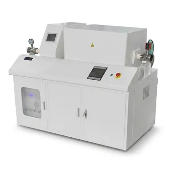
Chemical Vapor Deposition CVD System Slide PECVD Tube Furnace with Liquid Gasifier PECVD Machine
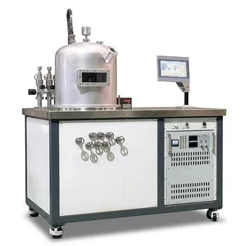
HFCVD Machine System for Nano Diamond Coating on Drawing Dies and Industrial Tools
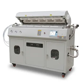
Multi Heating Zones CVD Tube Furnace System for Precision Chemical Vapor Deposition and Advanced Material Synthesis
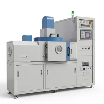
Radio Frequency Plasma Enhanced Chemical Vapor Deposition RF PECVD System for Laboratory and Industrial Thin Film Growth
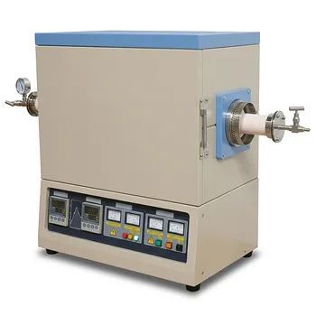
High Temperature 1700C Dual Zone Tube Furnace for Material Science and Industrial Chemical Vapor Deposition Research
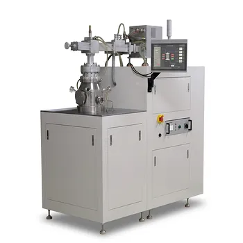
Cylindrical Resonator MPCVD Machine System for Microwave Plasma Chemical Vapor Deposition and Lab Diamond Growth
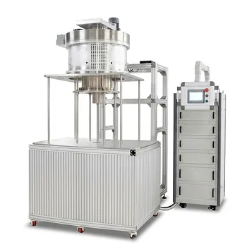
915MHz MPCVD Diamond Machine Microwave Plasma Chemical Vapor Deposition System Reactor
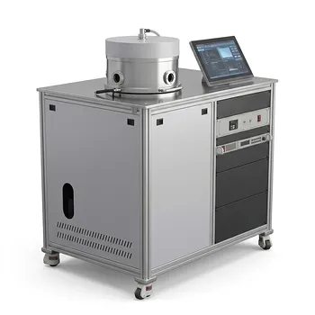
Inclined Rotary Plasma Enhanced Chemical Vapor Deposition PECVD System for Thin Film Deposition and Nanomaterial Synthesis
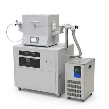
Split Chamber CVD Tube Furnace with Vacuum Station Chemical Vapor Deposition System Machine
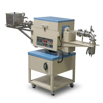
Two Zone Rotary CVD Furnace with Automatic Feeding and Receiving System for Powder Processing
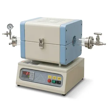
1200C Tube Furnace with Internal Magnetic Sample Sliding for Direct Vaporizing Deposition and Rapid Thermal Processing
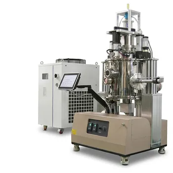
950C Rapid Thermal Processing Furnace for 12 Inch Wafer CSS Coating with Rotating Substrate Holder
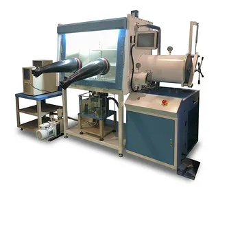
High Temperature Induction Melting System with Integrated Ultra High Purity Glove Box for Metallic Alloy Processing