What are the specific applications of tube furnaces in semiconductor fabrication and research? Lab Solutions for R&D
Updated 3 months ago
Tube furnaces are indispensable instruments in semiconductor fabrication and materials research. They are primarily utilized for diffusion doping, thermal oxidation of gate dielectrics, annealing, and Chemical Vapor Deposition (CVD) of thin films. By providing a sealed, high-temperature environment with exceptional thermal uniformity, these furnaces enable the simultaneous processing of multiple wafers while ensuring precise chemical and structural integrity.
The tube furnace serves as a controlled thermal reactor that allows for the precise modification of semiconductor materials at the atomic level. Its ability to maintain a stable, high-concentration gas environment while ensuring uniform heat distribution across a batch is critical for achieving consistent electronic properties.
Fundamental Processing Techniques
Diffusion Doping and Ion Activation
Tube furnaces are a primary tool for introducing impurities into a semiconductor lattice to alter its electrical conductivity. In this process, the furnace provides the high temperatures necessary for dopant atoms to migrate into the wafer surface.
This environment also facilitates the "activation" of these dopants. After ion implantation, a high-temperature annealing step in the furnace repairs the crystal lattice and moves the dopant atoms into substitutional sites where they can contribute to conductivity.
Thermal Oxidation for Dielectric Layers
A critical application is the growth of high-quality silicon dioxide (SiO2) layers, which serve as gate dielectrics or isolation layers. The tube furnace creates a high-concentration oxygen environment where the silicon surface reacts to form an oxide.
Because the furnace provides highly uniform radial heating, the resulting oxide layers are exceptionally even across the entire wafer batch. This uniformity is essential for maintaining consistent performance in modern integrated circuits.
Chemical Vapor Deposition (CVD)
Tube furnaces are frequently configured for CVD, where gaseous precursors react or decompose on the substrate surface to form thin films. This is used to deposit a variety of materials, including polysilicon, silicon nitride, and various oxides.
The sealed nature of the quartz or ceramic tube allows for the safe handling of hazardous precursors like silane or ammonia. These systems can be operated at atmospheric or low pressure to fine-tune the film's morphology and growth rate.
Specialized Research Applications
Precise Oxidation of 2D Materials
In advanced memristor research, such as the fabrication of Ag/TiOx/SnOx/SnSe2 devices, tube furnaces are used for "mild" thermal oxidation. By controlling temperatures precisely—often as low as 200°C—researchers can convert the surface of 2D materials like SnSe2 into ultra-thin oxide layers.
This controlled environment is the primary safeguard for achieving atomically smooth interfaces. Such precision is vital for the development of next-generation non-volatile memory and neuromorphic computing components.
Solid-State Reactions and Crystal Growth
Beyond wafer processing, tube furnaces are used to synthesize new materials through solid-state reactions. This involves heating mixed powders to high temperatures to trigger chemical transformations, which is essential for creating complex oxides and high-temperature superconductors.
Researchers also utilize "chemical vapor transport" within these furnaces to grow high-purity crystals. The furnace establishes a temperature gradient along the tube, allowing material to evaporate at one end and deposit as a crystal at the other.
Technical Advantages in Semiconductor Workflows
Batch Processing Efficiency
Unlike single-wafer rapid thermal processing (RTP) tools, tube furnaces excel at batch processing. The extended heated length of the tube allows dozens of wafers to be processed simultaneously under identical conditions.
This ensures high throughput and lowers the cost per wafer for processes that require long soak times. The cylindrical geometry naturally provides uniform heating to all wafers in the stack.
Atmospheric Control and Contamination Shielding
The furnace tube acts as a physical barrier that isolates the samples from the external environment and heating elements. This is critical for preventing metallic contamination that could ruin the electrical properties of the semiconductor.
Operators can precisely control the internal atmosphere, whether it requires a high-vacuum, an inert gas like argon, or a highly reactive chemical environment. This flexibility makes the tube furnace a versatile tool for both standard fabrication and experimental synthesis.
Understanding the Trade-offs
Thermal Mass and Cycle Times
One significant limitation of the tube furnace is its high thermal mass. Unlike lamp-based heating systems, tube furnaces take a considerable amount of time to heat up and cool down, making them less suitable for processes requiring ultra-fast thermal cycling.
Potential for Cross-Contamination
In a shared research environment, the interior of the furnace tube can become coated with residues from previous runs. If not properly managed through dedicated tubes for specific materials (e.g., separating "clean" oxidation from "dirty" doping), this can lead to cross-contamination between different batches.
How to Apply This to Your Project
Making the Right Choice for Your Goal
- If your primary focus is high-volume wafer production: Utilize the batch processing capabilities of the tube furnace for standard oxidation and diffusion steps to maximize throughput.
- If your primary focus is 2D material synthesis: Use a furnace with precise low-temperature control and a high-purity quartz tube to achieve the mild oxidation required for smooth interfaces.
- If your primary focus is crystal growth or sintering: Choose a multi-zone tube furnace that allows you to establish specific temperature gradients along the length of the tube.
- If your primary focus is depositing hazardous thin films: Ensure your furnace is integrated with a professional gas delivery and scrubbing system to safely manage precursors like silane.
The tube furnace remains a foundational technology in the semiconductor industry, bridging the gap between fundamental materials science and high-volume device manufacturing.
Summary Table:
| Application Category | Primary Process | Key Benefit for Semiconductors |
|---|---|---|
| Doping & Activation | Diffusion & Ion Activation | Ensures uniform electrical conductivity & lattice repair. |
| Dielectric Growth | Thermal Oxidation | Produces uniform, high-quality SiO2 gate dielectric layers. |
| Thin Film Growth | CVD (Chemical Vapor Deposition) | Enables safe, uniform deposition of polysilicon and nitrides. |
| Advanced Research | 2D Material Oxidation | Provides atomic-level precision for next-gen memristors. |
| Material Synthesis | Crystal Growth & Sintering | Multi-zone control for high-purity solid-state reactions. |
Elevate Your Semiconductor R&D with THERMUNITS Precision
As a global leader in high-temperature laboratory equipment, THERMUNITS understands that precision at the atomic level is non-negotiable for material science. Our comprehensive range of thermal processing solutions—including Tube, Muffle, Vacuum, Atmosphere, and Rotary furnaces, as well as CVD/PECVD systems—is engineered to provide the thermal uniformity and atmospheric control required for cutting-edge semiconductor fabrication.
Whether you are scaling batch production or exploring experimental 2D materials, our experts are ready to help you find the perfect heat treatment solution to accelerate your innovation.
Contact Our Engineering Team Today
Mentioned Products
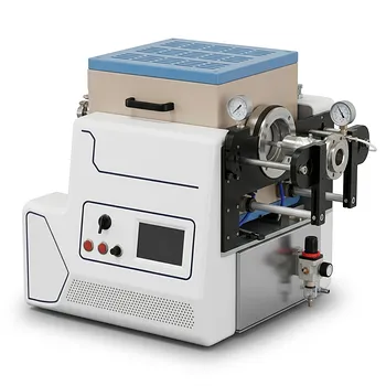
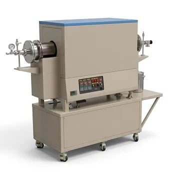
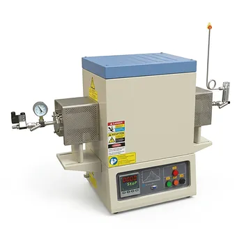
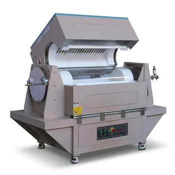
- High Temperature Tube Furnace 1500C with Sliding Flanges and 50mm OD for Rapid Thermal Processing Fast Heating and Cooling
- Vertical 1700C Vacuum and Atmosphere Tube Furnace with 80mm Alumina Tube
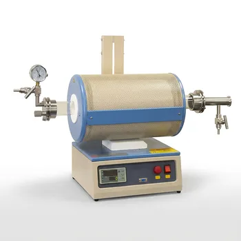
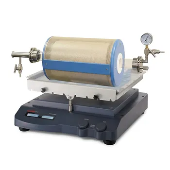
- Compact High Temperature 1600C Tube Furnace with 50mm Alumina Tube and Vacuum Flanges for Material Sintering
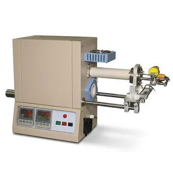
- 900°C Max Rotary Tube Furnace with 8 Inch 310S Alloy Tube and Optional Multi Zone Heating for Industrial Material Calcination
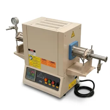
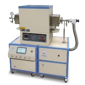
- 1100C Tube Furnace with Vacuum Flange and Programmable Temperature Controller for Material Science and Industrial Heat Treatment
People Also Ask
- Role of Tube Furnace in KNNLST Ceramic Synthesis: Achieve High Phase Purity and Thermal Uniformity
- How are high-temperature tube furnaces utilized to repair etching damage? Precision Lattice Restoration Solutions
- What is the function of a high-temperature tube furnace in NC support preparation? Achieve Precise Pyrolysis & Doping
- Why is post-deposition thermal treatment necessary for LiMn2O4 thin-film cathodes? Achieve Peak Battery Performance
- Why is an Argon protective atmosphere necessary within a high-temperature tube furnace during carbonization?
Tech Team · ThermUnits
Last updated on Apr 14, 2026
Related Products
High Temperature Tube Furnace 1500C with Sliding Flanges and 50mm OD for Rapid Thermal Processing Fast Heating and Cooling
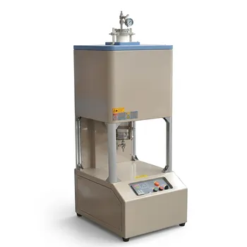
Vertical 1700C Vacuum and Atmosphere Tube Furnace with 80mm Alumina Tube
Compact High Temperature 1600C Tube Furnace with 50mm Alumina Tube and Vacuum Flanges for Material Sintering
900°C Max Rotary Tube Furnace with 8 Inch 310S Alloy Tube and Optional Multi Zone Heating for Industrial Material Calcination
1100C Tube Furnace with Vacuum Flange and Programmable Temperature Controller for Material Science and Industrial Heat Treatment
High Temperature 1700C Tube Furnace with High Vacuum Turbomolecular Pump System and Multi Channel Mass Flow Controller Gas Mixer
1700C Hydrogen Gas Tube Furnace with 60mm Alumina Process Tube and Integrated Hydrogen Safety Detector
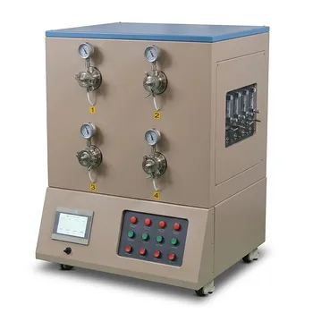
5 Inch Three Zone Rotary Tube Furnace with Integrated Gas Delivery System and 1200C Capability for Advanced Material CVD Processing
1200°C 5 Inch Vertical Quartz Tube Furnace with Stainless Steel Vacuum Flanges
High Temperature 1700C Six Zone Split Tube Furnace with Alumina Tube and Water Cooled Flanges
Compact Vertical Split Quartz Tube Furnace with Stainless Steel Vacuum Flanges for Rapid Thermal Quenching and Controlled Atmosphere Material Processing
1200C High Throughput Multi Channel Tube Furnace with 50mm Quartz Tubes for Annealing and Material Phase Diagram Research
High Vacuum Compact Tube Furnace 1200C with Integrated Turbo Pump System and 8 Inch Heating Zone
High Temperature 1700C Benchtop Tube Furnace with 5 Inch Heating Zone High Purity Alumina Tube and Vacuum Sealing Flanges
1800C High Temperature Compact Vacuum Tube Furnace with 60mm OD Alumina Tube and Kanthal MoSi2 Heating Elements
Three Zone Tube Furnace with 11 Inch or 15 Inch Quartz Tube and Hinged Flanges for Vacuum Atmosphere Heat Treatment
High Throughput 1200C Four Channel Tube Furnace with 3 Inch Quartz Tubes for Multi Zone Annealing and Material Research
High Temperature 1700C Vertical Tube Furnace for Powder Spherification and Material Sintering
High Temperature Rocking Tube Furnace with Quartz Tube and Vacuum Flange for Materials Synthesis