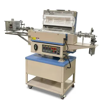
What are the technical benefits of using PECVD systems for SiNx layers? Superior Low-Temp Film Passivation
Updated 3 months ago
PECVD systems utilize plasma to drive chemical reactions at low temperatures, enabling the deposition of silicon nitride (SiNx) layers with precise optical and electronic properties. These systems allow for the creation of dense, uniform films that act as both anti-reflection coatings and passivation layers, which are critical for high-efficiency solar cells and semiconductor devices. By decoupling the energy required for the reaction from the substrate temperature, PECVD preserves the integrity of heat-sensitive materials while maintaining high film quality.
Core Takeaway: PECVD is the industry standard for SiNx deposition because it balances a low thermal budget with exceptional control over the film's refractive index and thickness, providing both superior optical performance and electrical passivation.
Superior Thermal Management and Substrate Protection
Operating at Reduced Temperatures
Unlike traditional thermal CVD, which requires temperatures between 600°C and 900°C, PECVD operates typically between 200°C and 400°C. This significant reduction in heat is achieved by using plasma to provide the activation energy necessary for chemical precursors like silane (SiH4) and ammonia (NH3) to react.
Preserving Sensitive Underlying Structures
The lower thermal budget is essential for protecting temperature-sensitive substrates, such as polymer films, glass, or pre-existing metal interconnects. This prevents unintended diffusion of dopants and minimizes the risk of thermal stress or mechanical distortion of the wafer.
Extending Equipment Longevity
Industrial PECVD systems avoid the physical damage to quartz furnace tubes and carriers that often occurs during high-temperature Low-Pressure CVD (LPCVD) processes. This reduction in hardware wear-and-tear leads to lower maintenance costs and higher uptime in large-scale production environments.
Precise Control of Optical and Physical Properties
Fine-Tuning the Refractive Index
PECVD equipment allows operators to precisely adjust the refractive index and thickness of the SiNx layer by varying gas flow ratios, pressure, and plasma power. This precision is vital for creating anti-reflection coatings (ARC) that maximize light absorption in solar cells or tune structural colors in optical filters.
Achieving High Film Uniformity
The system facilitates the uniform deposition of dielectric layers across large surface areas, with thickness control typically ranging from 30 nm to 130 nm. This consistency ensures that the optical and protective properties of the film are identical across the entire substrate, which is a requirement for high-yield manufacturing.
Dense and Pinhole-Free Film Growth
Compared to traditional evaporation methods, PECVD creates dense, pinhole-free films that offer superior environmental protection. These layers serve as effective moisture barriers and provide mechanical durability, enhancing the long-term reliability of the finished device.
Enhanced Electrical Passivation and Process Efficiency
Hydrogen-Induced Passivation
During the SiNx deposition process, hydrogen is often incorporated into the film, which facilitates surface and bulk passivation. This process neutralizes "dangling bonds" at the silicon interface, significantly increasing the open-circuit voltage (Voc) and overall efficiency of solar cells.
Prevention of the Wrap-Around Effect
Modern industrial PECVD systems support single-sided deposition, which effectively prevents the "wrap-around" effect where material is unintentionally deposited on the edges or back of the wafer. This is a distinct advantage over diffusion furnaces and certain LPCVD processes that require additional cleaning steps.
High Precursor Utilization
PECVD systems are designed for high silane (SiH4) utilization, ensuring that precursor gases are consumed efficiently during the reaction. This efficiency reduces material waste and lowers the cost-per-wafer, making it a highly economical choice for mass production.
Understanding the Trade-offs
Plasma-Induced Damage
While plasma enables low-temperature reactions, the energetic ions can sometimes cause physical damage to the substrate surface. If not carefully managed, this ion bombardment can create defects that might partially offset the benefits of passivation.
Film Stoichiometry and Stability
Films deposited via PECVD are generally non-stoichiometric (SiNx rather than pure Si3N4) and can contain significant amounts of hydrogen. While beneficial for passivation, high hydrogen content may lead to film instability or "bubbling" if the device undergoes subsequent high-temperature processing steps.
Equipment Complexity
PECVD systems are technically more complex than simple thermal or evaporation systems, requiring vacuum systems, RF generators, and complex gas delivery modules. This complexity results in a higher initial capital investment and requires specialized technical expertise for optimization.
How to Apply This to Your Project
PECVD is a versatile tool, but its application should be tailored to your specific performance requirements and thermal constraints.
- If your primary focus is solar cell efficiency: Prioritize PECVD for its hydrogen-induced passivation and its ability to create multilayer anti-reflection coatings that maximize photon capture.
- If your primary focus is protecting sensitive layers: Utilize PECVD’s low-temperature regime (below 300°C) to deposit dielectric barriers without damaging metal interconnects or organic substrates.
- If your primary focus is high-volume manufacturing: Leverage PECVD’s single-sided deposition capabilities and high precursor utilization to minimize process steps and reduce material costs.
By mastering the balance between plasma power and gas chemistry, you can leverage PECVD to create high-performance SiNx layers that meet rigorous optical and electronic standards.
Summary Table:
| Key Benefit | Technical Advantage | Primary Application |
|---|---|---|
| Low Temperature | Operates at 200°C-400°C | Protects heat-sensitive substrates & polymers |
| Optical Precision | Fine-tuned refractive index | Anti-reflection coatings (ARC) for solar cells |
| Electrical Passivation | Hydrogen-induced bond neutralization | Increasing solar cell open-circuit voltage (Voc) |
| Film Quality | Dense, pinhole-free, uniform growth | Moisture barriers and semiconductor dielectric layers |
| Process Efficiency | Single-sided deposition | Eliminates wrap-around effect and reduces waste |
Elevate Your Material Research with THERMUNITS Precision
Are you looking to achieve superior film quality and precise thermal control in your lab? THERMUNITS is a leading manufacturer of high-temperature laboratory equipment dedicated to advancing material science and industrial R&D.
From high-performance CVD/PECVD systems for advanced thin-film deposition to a comprehensive range of Muffle, Vacuum, Tube, and Rotary furnaces, we provide the tools necessary for cutting-edge heat treatment. Whether you require a Vacuum Induction Melting furnace (VIM), Dental Furnaces, or specialized Thermal Elements, our solutions are engineered for durability and accuracy.
Ready to optimize your thermal processing? Contact our expert team today to discuss your specific requirements and discover how THERMUNITS can empower your next breakthrough.
References
- Qinqin Wang, Jianning Ding. Effects on Metallization of n+-Poly-Si Layer for N-Type Tunnel Oxide Passivated Contact Solar Cells. DOI: 10.3390/ma17112747
Mentioned Products
- Inclined Rotary Plasma Enhanced Chemical Vapor Deposition PECVD System for Thin Film Deposition and Nanomaterial Synthesis
- Radio Frequency Plasma Enhanced Chemical Vapor Deposition RF PECVD System for Laboratory and Industrial Thin Film Growth
- Chemical Vapor Deposition CVD System Slide PECVD Tube Furnace with Liquid Gasifier PECVD Machine
- 1200C Max Compact Auto-Sliding PECVD Furnace with 2 Inch Tube and Vacuum Pump
- 915MHz MPCVD Diamond Machine Microwave Plasma Chemical Vapor Deposition System Reactor
People Also Ask
- What types of materials can be deposited using PECVD systems? Explore Versatile Thin-Film Coating Solutions
- How does the non-equilibrium nature of plasma facilitate low-temperature deposition in PECVD systems? Pro Tips for R&D
- How is Plasma-Enhanced Chemical Vapor Deposition (PECVD) utilized in the production of photovoltaic solar cells? Study
- How do RF frequency and power settings influence the characteristics of a PECVD process? Master Quality & Efficiency
- What are the advantages of PECVD systems for nano flame retardant films? Protect Heat-Sensitive Polymers with Precision

Tech Team · ThermUnits
Last updated on Jun 02, 2026
Related Products
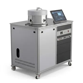
Inclined Rotary Plasma Enhanced Chemical Vapor Deposition PECVD System for Thin Film Deposition and Nanomaterial Synthesis
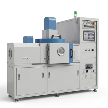
Radio Frequency Plasma Enhanced Chemical Vapor Deposition RF PECVD System for Laboratory and Industrial Thin Film Growth
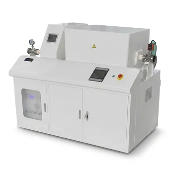
Chemical Vapor Deposition CVD System Slide PECVD Tube Furnace with Liquid Gasifier PECVD Machine
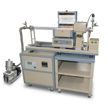
1200C Max Compact Auto-Sliding PECVD Furnace with 2 Inch Tube and Vacuum Pump
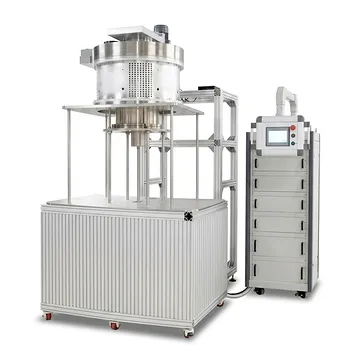
915MHz MPCVD Diamond Machine Microwave Plasma Chemical Vapor Deposition System Reactor
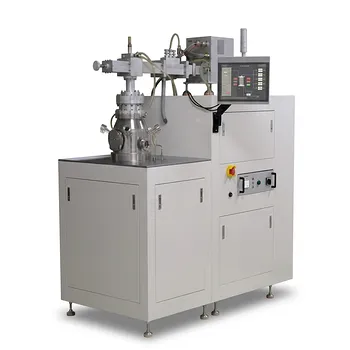
Cylindrical Resonator MPCVD Machine System for Microwave Plasma Chemical Vapor Deposition and Lab Diamond Growth
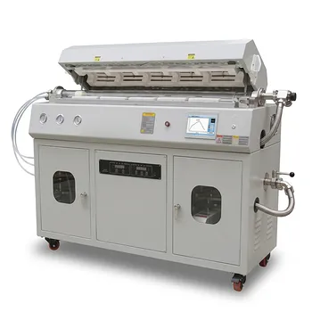
Multi Heating Zones CVD Tube Furnace System for Precision Chemical Vapor Deposition and Advanced Material Synthesis
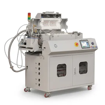
Versatile Chemical Vapor Deposition Tube Furnace System for Advanced Material Research and Industrial Coating Processes
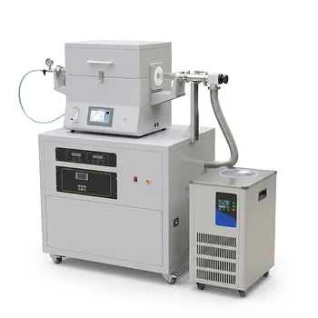
Split Chamber CVD Tube Furnace with Vacuum Station Chemical Vapor Deposition System Machine
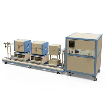
1200C Dual Sliding Tube Furnace with Dual Tubes and Flanges for PECVD Processes
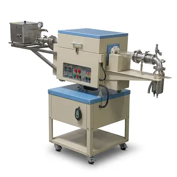
Two Zone Rotary CVD Furnace with Automatic Feeding and Receiving System for Powder Processing
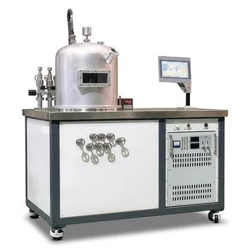
HFCVD Machine System for Nano Diamond Coating on Drawing Dies and Industrial Tools
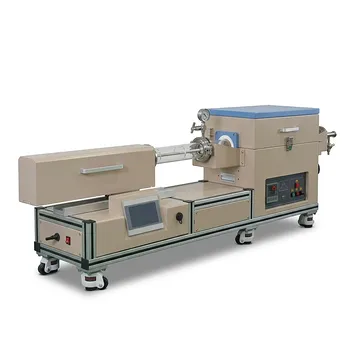
1200C Sliding Internal Crucible Tube Furnace for Controlled Atmosphere Thin Film Deposition and Material Sublimation Research
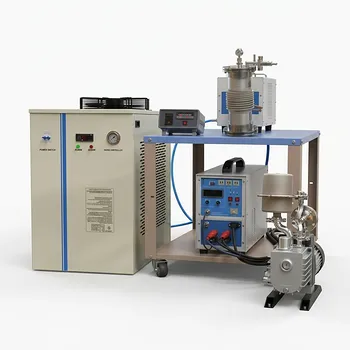
Induction Heating System with Temperature Control for High Temperature Vacuum Sintering and Melting