How is Plasma-Enhanced Chemical Vapor Deposition (PECVD) utilized in the production of photovoltaic solar cells? Study
Updated 5 months ago
Plasma-Enhanced Chemical Vapor Deposition (PECVD) is a cornerstone technology in solar manufacturing used to deposit thin films that maximize light absorption and minimize energy loss. Specifically, it is utilized to apply silicon nitride (SiNx) anti-reflective coatings and surface passivation layers that prevent electrons from being lost at the wafer surface. Beyond these standard coatings, PECVD is essential for depositing the functional silicon layers in high-efficiency architectures like Heterojunction (HJT) and TOPCon cells.
PECVD enables the high-speed deposition of high-quality dielectric and semiconductor films at low temperatures. This process is the primary hardware guarantee for achieving high photoelectric conversion efficiency by reducing both optical reflection and electronic recombination.
Enhancing Light Absorption and Electronic Quality
Reducing Surface Reflection
The most visible application of PECVD is the deposition of a silicon nitride (SiNx) anti-reflective coating (ARC) on the front of silicon wafers. This layer gives solar cells their characteristic blue color and ensures that more photons are captured by the cell rather than being reflected away.
Minimizing Recombination via Passivation
PECVD deposits hydrogen-rich films that chemically "passivate" the surface of the silicon wafer. This process neutralizes dangling bonds at the atomic level, which significantly reduces surface recombination velocity and allows more generated electrons to be collected as electricity.
Improving Minority Carrier Lifetime
By providing superior surface and bulk passivation, PECVD-deposited layers improve the minority carrier lifetime within the silicon. This directly leads to higher open-circuit voltages and overall energy conversion performance for the finished solar module.
Applications Across Modern Cell Architectures
Support for PERC and TOPCon Technologies
In mainstream PERC (Passivated Emitter and Rear Cell) and emerging TOPCon designs, PECVD is used to create complex passivation stacks. These stacks often involve layers of silicon dioxide (SiO2) or alumina (Al2O3) capped with silicon nitride to protect the rear surface and enhance internal reflection.
Enabling Heterojunction (HJT) Cells
For Heterojunction technology, PECVD is indispensable for depositing thin layers of intrinsic and doped amorphous silicon (a-Si). These layers create the junction of the cell at temperatures low enough to avoid damaging the high-quality monocrystalline silicon wafer.
Thin-Film and Tandem Solar Structures
In thin-film solar production, PECVD deposits the active semiconductor layers and transparent conductive oxide (TCO) underlayers. It is also becoming a critical tool for developing tandem PV technologies, where multiple layers are stacked to capture a broader spectrum of sunlight.
Technical Advantages of the Plasma Process
Operating at Lower Thermal Budgets
The defining advantage of PECVD is its ability to operate at substrate temperatures between 200°C and 400°C. Traditional thermal CVD requires 600°C to 900°C, which can cause unwanted diffusion or damage to temperature-sensitive structures and metal interconnects.
High-Throughput Production
PECVD systems are designed for high-volume manufacturing, capable of processing large-area or textured substrates uniformly. This scalability is essential for maintaining the cost-effectiveness required in the global solar market.
Precise Control of Film Chemistry
The use of RF or microwave-generated plasma allows for the precise dissociation of precursor gases. This gives manufacturers fine-tuned control over the refractive index, thickness, and hydrogen content of the deposited films.
Understanding the Trade-offs
Potential for Plasma-Induced Damage
While the plasma provides the energy for the reaction, the bombardment of the wafer surface by ions can occasionally cause lattice damage. This requires careful tuning of the plasma power and frequency to balance deposition speed with the electronic integrity of the wafer.
Equipment Complexity and Maintenance
PECVD systems are significantly more complex and expensive to maintain than simpler atmospheric pressure systems. The requirement for vacuum environments and the management of hazardous precursor gases like silane (SiH4) increases the operational overhead for manufacturers.
How to Apply PECVD Strategies to Your Project
Recommendations for Solar Manufacturing
Successful implementation of PECVD depends on aligning the deposition parameters with the specific requirements of your cell architecture.
- If your primary focus is maximizing efficiency in HJT cells: Prioritize PECVD systems that offer extremely precise control over amorphous silicon thickness and interface purity to minimize carrier transport losses.
- If your primary focus is high-volume PERC or TOPCon production: Focus on high-throughput PECVD tools that can deliver uniform silicon nitride coatings across thousands of wafers per hour with minimal downtime for chamber cleaning.
- If your primary focus is emerging Tandem PV research: Utilize PECVD's flexibility to experiment with different transparent conductive oxides and doped layers that require low-temperature processing to protect the underlying perovskite or silicon layers.
By mastering PECVD, manufacturers can precisely tune the optical and electronic properties of solar cells to reach the theoretical limits of photovoltaic efficiency.
Summary Table:
| Application | Core Function | Impact on Performance |
|---|---|---|
| Anti-Reflective Coating | Deposits SiNx thin films | Minimizes photon reflection, increasing light absorption. |
| Surface Passivation | Neutralizes dangling bonds | Reduces recombination velocity for higher carrier collection. |
| HJT/TOPCon Layers | Deposits a-Si and dielectric stacks | Enables high-efficiency junctions at low thermal budgets. |
| Low-Temp Deposition | Operates at 200°C - 400°C | Protects sensitive substrates and metal interconnects. |
Maximize Your Solar Efficiency with THERMUNITS
As a leading manufacturer of high-temperature laboratory equipment for material science and industrial R&D, THERMUNITS provides the precision hardware necessary to master PECVD and other critical thermal processes. Whether you are scaling PERC/TOPCon production or researching next-generation HJT and Tandem PV architectures, our comprehensive range of thermal solutions—including advanced CVD/PECVD systems, Vacuum, Tube, and Atmosphere furnaces, as well as VIM and Rotary Kilns—ensures superior film quality and repeatable results.
Ready to optimize your photovoltaic research? Contact THERMUNITS experts today to find the ideal heat treatment equipment for your specific R&D or manufacturing needs.
Mentioned Products
- Inclined Rotary Plasma Enhanced Chemical Vapor Deposition PECVD System for Thin Film Deposition and Nanomaterial Synthesis
- Radio Frequency Plasma Enhanced Chemical Vapor Deposition RF PECVD System for Laboratory and Industrial Thin Film Growth
- Chemical Vapor Deposition CVD System Slide PECVD Tube Furnace with Liquid Gasifier PECVD Machine
- 1200C Max Compact Auto-Sliding PECVD Furnace with 2 Inch Tube and Vacuum Pump
- 1200C Dual Sliding Tube Furnace with Dual Tubes and Flanges for PECVD Processes
People Also Ask
- What types of materials can be deposited using PECVD systems? Explore Versatile Thin-Film Coating Solutions
- How does the non-equilibrium nature of plasma facilitate low-temperature deposition in PECVD systems? Pro Tips for R&D
- How do RF frequency and power settings influence the characteristics of a PECVD process? Master Quality & Efficiency
- What are the advantages of PECVD systems for nano flame retardant films? Protect Heat-Sensitive Polymers with Precision
- What are the benefits of using PECVD for optical and photonic coatings? Achieve High-Precision Thin-Film Deposition

Tech Team · ThermUnits
Last updated on Apr 14, 2026
Related Products
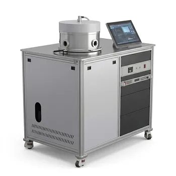
Inclined Rotary Plasma Enhanced Chemical Vapor Deposition PECVD System for Thin Film Deposition and Nanomaterial Synthesis
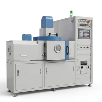
Radio Frequency Plasma Enhanced Chemical Vapor Deposition RF PECVD System for Laboratory and Industrial Thin Film Growth
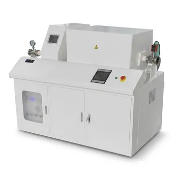
Chemical Vapor Deposition CVD System Slide PECVD Tube Furnace with Liquid Gasifier PECVD Machine
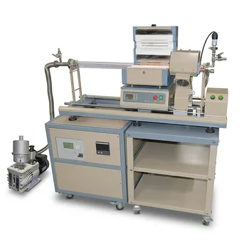
1200C Max Compact Auto-Sliding PECVD Furnace with 2 Inch Tube and Vacuum Pump
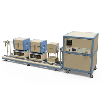
1200C Dual Sliding Tube Furnace with Dual Tubes and Flanges for PECVD Processes
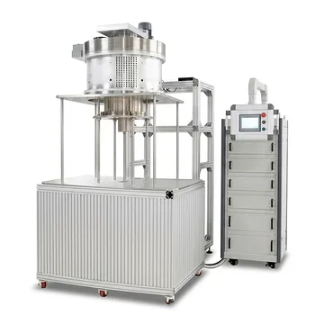
915MHz MPCVD Diamond Machine Microwave Plasma Chemical Vapor Deposition System Reactor
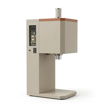
Vertical Openable Tube Furnace 0-1700c High Temperature Laboratory System for CVD and Vacuum Heat Treatment
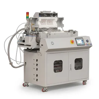
Versatile Chemical Vapor Deposition Tube Furnace System for Advanced Material Research and Industrial Coating Processes
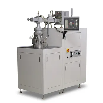
Cylindrical Resonator MPCVD Machine System for Microwave Plasma Chemical Vapor Deposition and Lab Diamond Growth
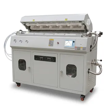
Multi Heating Zones CVD Tube Furnace System for Precision Chemical Vapor Deposition and Advanced Material Synthesis
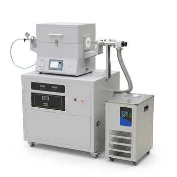
Split Chamber CVD Tube Furnace with Vacuum Station Chemical Vapor Deposition System Machine
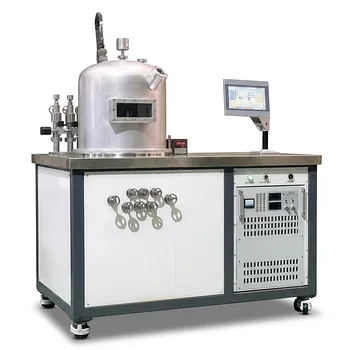
HFCVD Machine System for Nano Diamond Coating on Drawing Dies and Industrial Tools
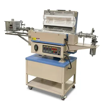
5 Inch Rotary Tube Furnace with Automatic Feeding and Receiving System 1200C Three Zone CVD Powder Processing
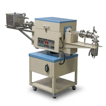
Two Zone Rotary CVD Furnace with Automatic Feeding and Receiving System for Powder Processing
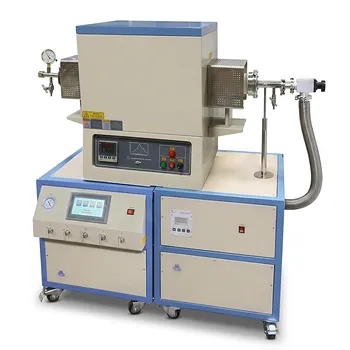
High Temperature 1700C Tube Furnace with High Vacuum Turbomolecular Pump System and Multi Channel Mass Flow Controller Gas Mixer
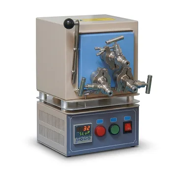
Triple Tube Compact Hybrid Muffle Furnace 1000C High Vacuum Thermal Processing System
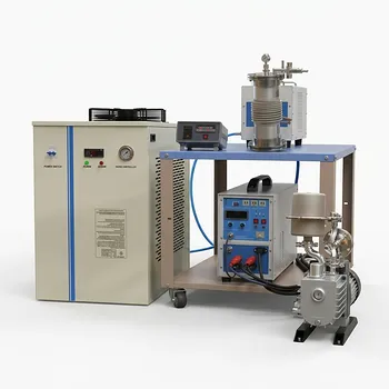
Induction Heating System with Temperature Control for High Temperature Vacuum Sintering and Melting
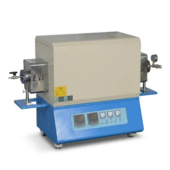
High Temperature Dual Zone Vacuum Tube Furnace for Material Research and CVD Processing
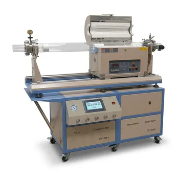
Dual Tube 100mm 80mm CVD Sliding Furnace with 4 Channel Gas Mixing and Vacuum System