What are the specific advantages of using PECVD compared to thermal CVD? Low-Temp Solutions for Thin-Film Growth
Updated 3 months ago
Plasma-Enhanced Chemical Vapor Deposition (PECVD) provides a critical "low-temperature" pathway for thin-film growth. Unlike traditional thermal CVD, which requires 600°C to 900°C, PECVD operates between room temperature and 400°C. This drastic reduction in thermal energy allows for high-quality deposition on heat-sensitive substrates like polymers and pre-processed metal layers without causing thermal damage or unintended material diffusion.
PECVD leverages non-thermal plasma energy to dissociate precursor gases, enabling the fabrication of high-performance films at temperatures that would otherwise melt or degrade modern semiconductor and flexible electronic components.
Preservation of Heat-Sensitive Architectures
Protection of Underlayer Structures
The primary advantage of PECVD is its low thermal budget, which is essential for protecting underlying layers. High-temperature thermal CVD can cause unintended diffusion of dopants or damage existing metal interconnects (such as aluminum) that have low melting points.
Compatibility with Polymers and Glass
Because PECVD can operate at temperatures as low as 100°C, it is the preferred method for depositing films on polymer substrates and heat-sensitive glass. This capability is vital for flexible electronics and optical coatings where thermal expansion or melting would destroy the substrate.
Maintaining Intrinsic Material Properties
PECVD allows for the growth of advanced materials, such as vertically aligned graphene, while preserving their intrinsic thermal and electrical properties. By avoiding the extreme heat of thermal processes, the system prevents thermal resistance caused by defects and sheet interfaces.
Enhanced Control and Film Quality
Superior Optical Tuning
PECVD offers precise control over the refractive index and film thickness, making it ideal for multi-layer optical stacks. Designers can tune these properties for broadband anti-reflection or high-reflectivity coatings that remain transparent and distortion-free.
Dense and Pinhole-Free Films
The plasma-driven reaction creates dense, pinhole-free films that provide better environmental protection than traditional evaporation methods. These films serve as excellent passivation layers (such as silicon nitride) that protect sensitive electronic circuits from moisture and contaminants.
Direct Growth of Nanostructures
The energetic nature of the plasma enables the bottom-up fabrication of complex structures like vertical graphene frameworks. This provides a significant advantage over top-down methods by reducing defects and improving the mechanical durability of the resulting material.
Industrial and Process Efficiencies
Prevention of the Wrap-Around Effect
Industrial PECVD systems often support single-sided deposition, which is a major advantage in semiconductor manufacturing. This prevents the wrap-around effect—where material deposits on the back of the wafer—common in high-temperature diffusion furnaces.
High Precursor Utilization
PECVD systems are designed for high silane (SiH4) utilization, making the process more cost-effective for large-scale production. Reactive species are generated more efficiently through electron-impact dissociation rather than relying solely on heat.
Equipment Longevity
Operating at lower temperatures reduces the physical damage and stress on quartz furnace tubes and carriers. This results in lower maintenance costs and longer equipment lifespans compared to Low-Pressure CVD (LPCVD) processes, which cause significant thermal wear over time.
Understanding the Trade-offs
The Risk of Plasma Damage
A significant pitfall of PECVD is potential ion bombardment damage to the substrate surface. The energetic species in the plasma can create surface defects that may negatively impact the electrical performance of highly sensitive semiconductor devices.
Film Purity and Incorporation
Because PECVD operates at lower temperatures, the chemical reactions may be less complete than in thermal CVD. This can lead to the unwanted incorporation of hydrogen or other precursor fragments into the film, potentially affecting the material's long-term stability or chemical resistance.
Complexity and Cost
PECVD systems are generally more mechanically complex than simple thermal reactors. The requirement for vacuum systems, RF (Radio Frequency) power generators, and precise gas flow controllers often translates to a higher initial capital investment.
Applying PECVD to Your Project
Recommendations for Material Processing
- If your primary focus is processing temperature-sensitive materials (like polymers or aluminum): Use PECVD to keep substrate temperatures below 400°C and prevent melting or thermal degradation.
- If your primary focus is creating high-performance optical coatings: Leverage PECVD for its ability to precisely tune refractive indices and produce dense, durable anti-reflective layers.
- If your primary focus is maximizing throughput in a semiconductor line: Utilize PECVD’s single-sided deposition capabilities to eliminate the need for backside cleaning and reduce processing steps.
- If your primary focus is achieving the highest possible film purity: Consider thermal CVD (if the substrate can withstand it), as higher temperatures often result in fewer precursor impurities and better stoichiometry.
By decoupling the energy needed for chemical reactions from the substrate's temperature, PECVD serves as the indispensable bridge between high-performance thin-film quality and the delicate requirements of modern material science.
Summary Table:
| Feature | Plasma-Enhanced CVD (PECVD) | Thermal CVD |
|---|---|---|
| Operating Temperature | Low (Room Temp to 400°C) | High (600°C to 900°C+) |
| Substrate Compatibility | Polymers, Glass, Aluminum, Flexible Electronics | High-temp ceramics, Refractory metals |
| Film Characteristics | Dense, pinhole-free, tunable refractive index | High purity, excellent stoichiometry |
| Process Benefit | Single-sided deposition, high gas utilization | Uniformity on complex 3D shapes |
| Thermal Budget | Low (Protects underlying structures) | High (Risk of dopant diffusion/melting) |
Optimize Your Thin-Film Research with THERMUNITS
Are you looking to achieve high-quality thin-film deposition without compromising heat-sensitive substrates? THERMUNITS is a leading manufacturer of advanced high-temperature laboratory equipment tailored for material science and industrial R&D. We offer specialized CVD/PECVD systems designed for precision and efficiency.
Our comprehensive range of thermal processing solutions includes:
- Laboratory Furnaces: Muffle, Vacuum, Atmosphere, Tube, and Rotary Furnaces.
- Advanced Systems: CVD/PECVD, Vacuum Induction Melting (VIM), and Hot Press Furnaces.
- Specialized Equipment: Dental Furnaces, Electric Rotary Kilns, and high-quality Thermal Elements.
Whether you are developing flexible electronics or advanced optical coatings, our experts are ready to help you select the ideal heat treatment equipment.
Contact THERMUNITS Today for a Professional Consultation
Mentioned Products
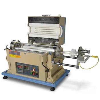
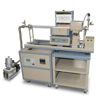
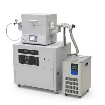
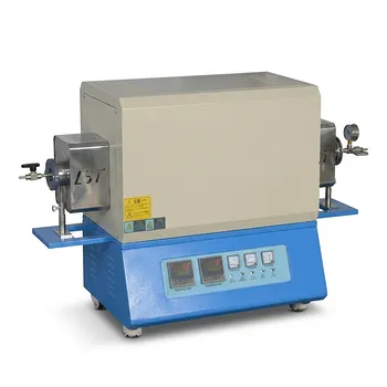
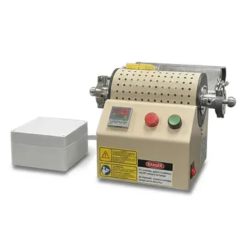
- Chemical Vapor Deposition CVD System Slide PECVD Tube Furnace with Liquid Gasifier PECVD Machine
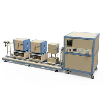
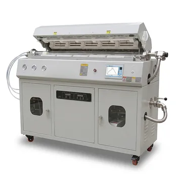
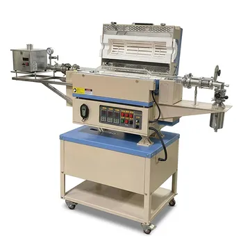
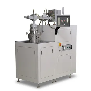
- Inclined Rotary Plasma Enhanced Chemical Vapor Deposition PECVD System for Thin Film Deposition and Nanomaterial Synthesis
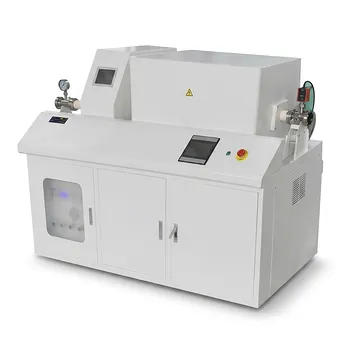
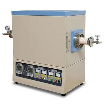
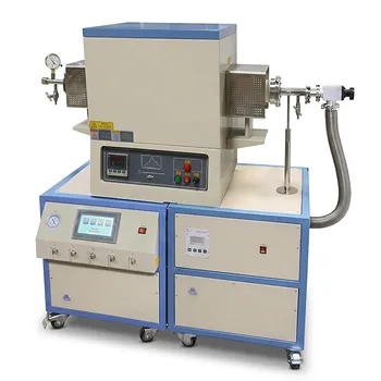
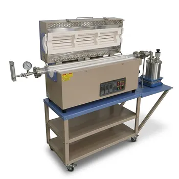
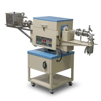
- Radio Frequency Plasma Enhanced Chemical Vapor Deposition RF PECVD System for Laboratory and Industrial Thin Film Growth
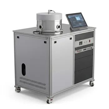
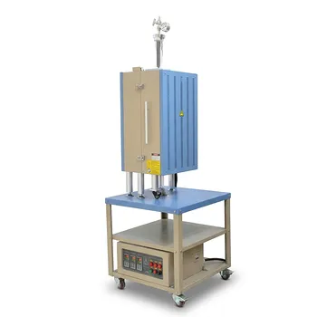
- 1200C Max Compact Auto-Sliding PECVD Furnace with 2 Inch Tube and Vacuum Pump
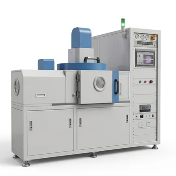
- 1200C Dual Sliding Tube Furnace with Dual Tubes and Flanges for PECVD Processes
People Also Ask
- What is the primary technical difference between PECVD and conventional thermal CVD? Understanding Energy & Temperature
- What are the primary applications and benefits of PECVD in modern micro- and nano-fabrication? Boost Thin Film Quality
- What role do by-product desorption and evacuation play in CVD film quality? Key Factors for High-Purity Films
- How do temperature regimes influence the growth rate of films in a CVD system? Master CVD Kinetics for Superior Thin Films
- What is the role of CVD/PECVD systems in the research of optoelectronic materials and functional coatings? Expert Guide
Tech Team · ThermUnits
Last updated on Apr 14, 2026
Related Products
Chemical Vapor Deposition CVD System Slide PECVD Tube Furnace with Liquid Gasifier PECVD Machine
Inclined Rotary Plasma Enhanced Chemical Vapor Deposition PECVD System for Thin Film Deposition and Nanomaterial Synthesis
Radio Frequency Plasma Enhanced Chemical Vapor Deposition RF PECVD System for Laboratory and Industrial Thin Film Growth
1200C Max Compact Auto-Sliding PECVD Furnace with 2 Inch Tube and Vacuum Pump
1200C Dual Sliding Tube Furnace with Dual Tubes and Flanges for PECVD Processes
High Temperature 1700C Dual Zone Tube Furnace for Material Science and Industrial Chemical Vapor Deposition Research
Vertical Openable Tube Furnace 0-1700c High Temperature Laboratory System for CVD and Vacuum Heat Treatment
Split Chamber CVD Tube Furnace with Vacuum Station Chemical Vapor Deposition System Machine
High Temperature 1700C Tube Furnace with High Vacuum Turbomolecular Pump System and Multi Channel Mass Flow Controller Gas Mixer
Multi Heating Zones CVD Tube Furnace System for Precision Chemical Vapor Deposition and Advanced Material Synthesis
915MHz MPCVD Diamond Machine Microwave Plasma Chemical Vapor Deposition System Reactor
High Temperature Dual Zone Vacuum Tube Furnace for Material Research and CVD Processing
5 Inch Rotary Tube Furnace with Automatic Feeding and Receiving System 1200C Three Zone CVD Powder Processing
1100°C Dual Zone Split Vertical Tube Furnace with 4 Inch Quartz Tube and Vacuum Sealing Flanges
5 Inch Two Zone Rotary Tube Furnace 1100C for Powder CVD and Material Synthesis
1000C Mini Tube Furnace with 20mm Quartz Tube and Vacuum Flanges for Material Science Research and Controlled Atmosphere Small Sample Processing
Cylindrical Resonator MPCVD Machine System for Microwave Plasma Chemical Vapor Deposition and Lab Diamond Growth
Two Zone Rotary CVD Furnace with Automatic Feeding and Receiving System for Powder Processing
1200C Three Zone Vertical Tube Furnace with 2 Inch Quartz Tube and Vacuum Flanges