How does Inductively Coupled Plasma (ICP) differ from Capacitively Coupled Plasma (CCP) in PECVD variants? Key Comparison
Updated 5 months ago
The fundamental difference between ICP and CCP lies in the mechanism of energy transfer and the resulting plasma density. While Capacitively Coupled Plasma (CCP) relies on electric fields between parallel electrodes, Inductively Coupled Plasma (ICP) uses electromagnetic induction to generate a plasma that is significantly denser and operates at lower pressures. This technical distinction determines whether a process is better suited for standard flat-film deposition or complex, high-aspect-ratio structural growth.
Core Takeaway: CCP is the reliable standard for uniform, parallel-plate deposition, but ICP provides the high-density environment ($>10^{11} \text{ cm}^{-3}$) necessary for high-speed growth and the filling of complex, deep-set microscopic features.
The Mechanics of Plasma Generation
CCP: The Parallel-Plate Standard
In a Capacitively Coupled Plasma (CCP) system, the plasma is generated between two parallel electrodes. An oscillating electric field is applied, which accelerates electrons back and forth to sustain the plasma.
This configuration is the traditional standard for PECVD due to its relative simplicity. It excels at providing a stable environment for uniform thin-film deposition over large areas.
ICP: Induction via External Coils
Inductively Coupled Plasma (ICP) systems utilize an external high-frequency induction coil to couple energy into the chamber. This creates a magnetic field that induces a current within the gas, ionizing it more efficiently than an electric field alone.
By decoupling the plasma generation from the substrate electrodes, ICP allows for independent control of plasma density and ion energy. This flexibility is a primary reason for its adoption in advanced fabrication.
Performance and Density Advantages
Achieving High Plasma Density
The most significant technical advantage of ICP is its ability to reach plasma densities exceeding $10^{11}$ particles per cubic centimeter. This is an order of magnitude higher than what is typically achievable in standard CCP configurations.
Higher density leads to a more efficient decomposition of precursor gases, such as methane. This efficiency allows for faster deposition rates and the formation of complex structures at relatively low substrate temperatures.
Low-Pressure Operation
ICP systems operate effectively at lower operating pressures than CCP systems. Lower pressure increases the "mean free path" of particles, meaning they travel further before colliding with others.
This characteristic is vital for filling high-aspect-ratio features in semiconductor and MEMS fabrication. The particles can penetrate deep into narrow trenches without being deflected by premature collisions.
Advanced Structural Applications
Specialized Growth and Carbon Nanowalls
The high-activity environment of ICP-PECVD provides the necessary energy and momentum for specialized growth, such as vertically oriented graphene. This enables the creation of Carbon Nanowalls, which require highly directed growth conditions.
In these applications, the ICP plasma provides the specific energy levels needed to break molecular bonds in precursors effectively. This results in the high-quality, few-layer structures required for modern nanotechnology.
Thermal Management in ICP
Because the plasma in an ICP system is so active, it can sustain the necessary chemical reactions at lower external temperatures. This makes it the preferred choice for depositing films on temperature-sensitive substrates that would otherwise be damaged in a high-heat environment.
Understanding the Trade-offs
Complexity and System Cost
The primary drawback of ICP-PECVD is the increased complexity of the hardware. Induction coils and the power supplies required to drive them are generally more expensive and harder to maintain than simple parallel-plate electrodes.
Uniformity Challenges
While CCP provides excellent broad-area uniformity, ICP can sometimes suffer from non-uniformity across very large wafers. The magnetic fields generated by the coils must be carefully engineered to ensure the plasma remains consistent across the entire processing area.
Choosing the Right Variant for Your Application
Selecting between CCP and ICP depends entirely on the geometric and thermal requirements of your specific device architecture.
- If your primary focus is standard thin-film uniformity: CCP-PECVD remains the most cost-effective and reliable choice for flat, non-complex layers.
- If your primary focus is high-aspect-ratio features: ICP-PECVD is essential for ensuring that deep trenches and holes are filled without voids or defects.
- If your primary focus is low-temperature carbon structures: ICP-PECVD provides the high-density plasma required to grow Carbon Nanowalls or graphene without overheating the substrate.
By matching the plasma generation method to your structural needs, you ensure both process efficiency and device integrity.
Summary Table:
| Feature | CCP (Capacitively Coupled) | ICP (Inductively Coupled) |
|---|---|---|
| Energy Transfer | Electric field (Parallel plates) | Electromagnetic induction (Coils) |
| Plasma Density | Moderate ($\approx 10^9 \text{ cm}^{-3}$) | High ($> 10^{11} \text{ cm}^{-3}$) |
| Operating Pressure | Higher | Lower (Increased mean free path) |
| Primary Strength | Uniformity for flat surfaces | High-speed growth & 3D features |
| Best Used For | Standard thin-film deposition | Carbon nanowalls, MEMS, deep trenches |
| System Complexity | Low (Cost-effective) | High (Advanced hardware) |
Optimize Your Research with Advanced PECVD Solutions
Are you looking to achieve superior film quality or develop complex nanostructures? THERMUNITS is a leading manufacturer of high-performance thermal processing equipment for material science and industrial R&D. We provide the precision tools necessary for cutting-edge semiconductor and material research.
Our comprehensive range includes:
- Advanced CVD/PECVD Systems for carbon nanotubes, graphene, and thin films.
- High-Temperature Furnaces: Muffle, Vacuum, Atmosphere, Tube, and Rotary variants.
- Specialized Equipment: Hot Press furnaces, VIM systems, and Dental Furnaces.
Unlock the full potential of your lab's R&D capabilities. Our experts are ready to help you select the ideal plasma configuration for your specific application.
Contact THERMUNITS Today to Get a Quote
Mentioned Products
- Inclined Rotary Plasma Enhanced Chemical Vapor Deposition PECVD System for Thin Film Deposition and Nanomaterial Synthesis
- Radio Frequency Plasma Enhanced Chemical Vapor Deposition RF PECVD System for Laboratory and Industrial Thin Film Growth
- Chemical Vapor Deposition CVD System Slide PECVD Tube Furnace with Liquid Gasifier PECVD Machine
- 1200C Max Compact Auto-Sliding PECVD Furnace with 2 Inch Tube and Vacuum Pump
- 1200C Dual Sliding Tube Furnace with Dual Tubes and Flanges for PECVD Processes
People Also Ask
- What types of materials can be deposited using PECVD systems? Explore Versatile Thin-Film Coating Solutions
- How does the non-equilibrium nature of plasma facilitate low-temperature deposition in PECVD systems? Pro Tips for R&D
- How is Plasma-Enhanced Chemical Vapor Deposition (PECVD) utilized in the production of photovoltaic solar cells? Study
- How do RF frequency and power settings influence the characteristics of a PECVD process? Master Quality & Efficiency
- What are the advantages of PECVD systems for nano flame retardant films? Protect Heat-Sensitive Polymers with Precision

Tech Team · ThermUnits
Last updated on Apr 14, 2026
Related Products
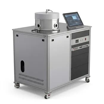
Inclined Rotary Plasma Enhanced Chemical Vapor Deposition PECVD System for Thin Film Deposition and Nanomaterial Synthesis
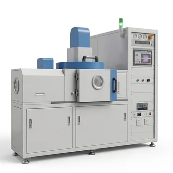
Radio Frequency Plasma Enhanced Chemical Vapor Deposition RF PECVD System for Laboratory and Industrial Thin Film Growth
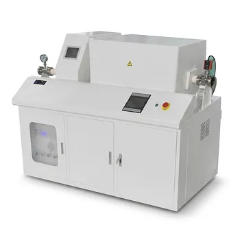
Chemical Vapor Deposition CVD System Slide PECVD Tube Furnace with Liquid Gasifier PECVD Machine
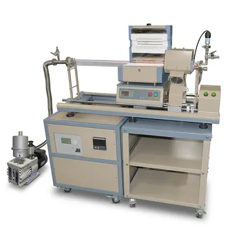
1200C Max Compact Auto-Sliding PECVD Furnace with 2 Inch Tube and Vacuum Pump
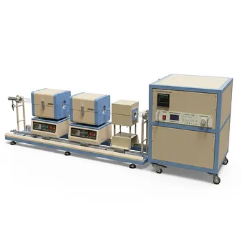
1200C Dual Sliding Tube Furnace with Dual Tubes and Flanges for PECVD Processes
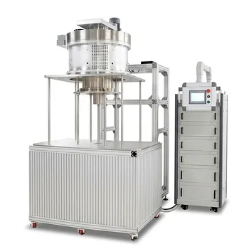
915MHz MPCVD Diamond Machine Microwave Plasma Chemical Vapor Deposition System Reactor
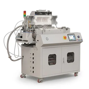
Versatile Chemical Vapor Deposition Tube Furnace System for Advanced Material Research and Industrial Coating Processes
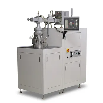
Cylindrical Resonator MPCVD Machine System for Microwave Plasma Chemical Vapor Deposition and Lab Diamond Growth
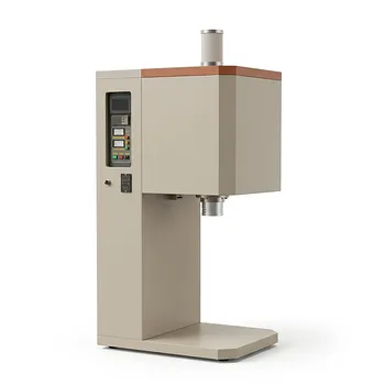
Vertical Openable Tube Furnace 0-1700c High Temperature Laboratory System for CVD and Vacuum Heat Treatment
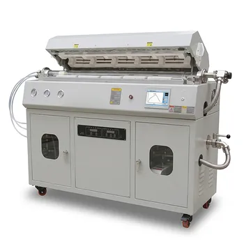
Multi Heating Zones CVD Tube Furnace System for Precision Chemical Vapor Deposition and Advanced Material Synthesis
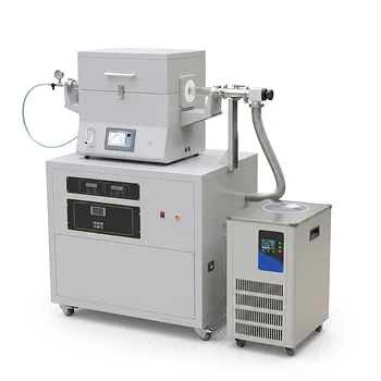
Split Chamber CVD Tube Furnace with Vacuum Station Chemical Vapor Deposition System Machine
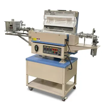
5 Inch Rotary Tube Furnace with Automatic Feeding and Receiving System 1200C Three Zone CVD Powder Processing
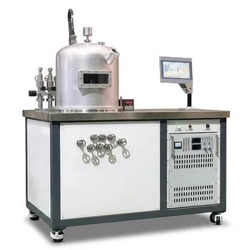
HFCVD Machine System for Nano Diamond Coating on Drawing Dies and Industrial Tools
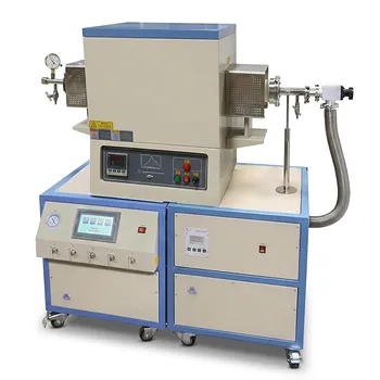
High Temperature 1700C Tube Furnace with High Vacuum Turbomolecular Pump System and Multi Channel Mass Flow Controller Gas Mixer
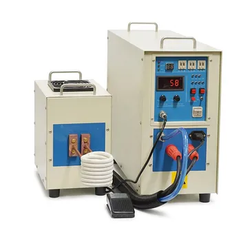
High Frequency Desktop Induction Heater 15 KVA Induction Heating System with Automatic Timer Control for Material Research and Metal Melting
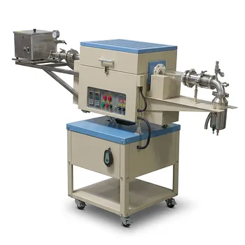
Two Zone Rotary CVD Furnace with Automatic Feeding and Receiving System for Powder Processing
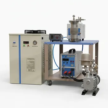
Induction Heating System with Temperature Control for High Temperature Vacuum Sintering and Melting
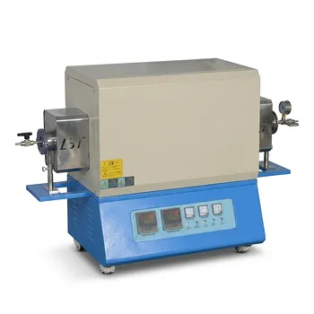
High Temperature Dual Zone Vacuum Tube Furnace for Material Research and CVD Processing
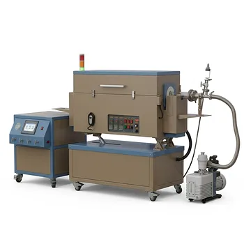
5 Inch Three Zone Rotary Tube Furnace with Integrated Gas Delivery System and 1200C Capability for Advanced Material CVD Processing