How does PECVD facilitate STO in LED fabrication? High-Density Masking for Precision InGaN Micro-LEDs
Updated 3 months ago
PECVD equipment facilitates Selective Thermal Oxidation (STO) by serving as the primary masking mechanism. It deposits a highly dense, microscopic layer of silicon dioxide ($SiO_2$) that acts as a chemical barrier against oxygen penetration. This precision-applied mask ensures that specific pixel areas are shielded from oxidation during high-temperature annealing, preserving the structural and functional integrity of sensitive InGaN green micro-LEDs.
The core value of PECVD in the STO process lies in its ability to deposit high-density protective films at low temperatures. These films act as temporary or permanent "oxygen blocks," allowing manufacturers to oxidize only the exposed regions of an LED structure while maintaining the light-emitting performance of the protected pixels.
The Role of the PECVD-Deposited $SiO_2$ Mask
Creating a Dense Oxygen Barrier
The primary function of PECVD equipment in this context is the deposition of a highly dense $SiO_2$ thin film. This density is critical because the film must have a microscopic structure tight enough to physically block oxygen molecules from diffusing through to the semiconductor surface.
Enabling Selective Oxidation
By patterning this $SiO_2$ layer, engineers can define which areas of the LED will undergo thermal oxidation and which will remain protected. This selective control is what allows for the creation of complex micro-LED architectures without damaging the active light-emitting regions.
Preserving Pixel Functionality
In InGaN green micro-LEDs, maintaining the stoichiometry and crystal structure is essential for color accuracy and efficiency. The PECVD mask ensures that the covered pixels remain unaffected by high-temperature annealing, preventing unintended chemical changes that would degrade light output.
The Advantage of Low-Temperature Processing
Managing the Thermal Budget
Traditional thermal CVD requires temperatures between 600°C and 900°C, which can damage sensitive LED layers or metal interconnects. PECVD utilizes plasma to activate precursor gases, allowing high-quality film deposition at significantly lower temperatures, typically between 200°C and 400°C.
Protecting Sensitive Materials
The lower thermal budget of PECVD is vital for preserving temperature-sensitive underlying structures. This is particularly important in micro-LED fabrication, where the high heat of traditional CVD could cause unwanted diffusion or thermal stress in the InGaN layers.
Maintaining Film Conformality
PECVD systems produce conformal thin films, meaning the $SiO_2$ mask wraps evenly around the three-dimensional structures of the micro-LED pixels. This uniform coverage is necessary to ensure that oxygen cannot "leak" in through the sidewalls of the pixels during the STO process.
Understanding the Trade-offs
Film Density vs. Internal Stress
While high-density films provide better oxygen blocking, they can also introduce mechanical stress into the LED wafer. If the PECVD parameters are not perfectly balanced, a mask that is too dense may cause the thin semiconductor layers to warp or crack.
Deposition Rate vs. Film Quality
Increasing the plasma power can lead to faster deposition rates, which is better for industrial throughput. However, faster growth can sometimes lead to porous films that fail to effectively block oxygen during the Selective Thermal Oxidation phase.
Potential for Hydrogen Incorporation
Because PECVD precursors often contain hydrogen (such as silane), some hydrogen may be trapped within the $SiO_2$ film. At the high temperatures used in the STO annealing process, this hydrogen could potentially migrate, affecting the electrical properties of the LED if the process is not carefully controlled.
How to Apply PECVD to Your Fabrication Goal
If you are integrating PECVD into an LED production line for Selective Thermal Oxidation, consider these strategic approaches based on your specific requirements:
- If your primary focus is Maximum Pixel Protection: Prioritize film density over deposition speed by optimizing plasma frequency and precursor ratios to ensure a leak-proof $SiO_2$ barrier.
- If your primary focus is Thermal Sensitivity: Utilize the lowest possible substrate temperature (near 200°C) and rely on higher RF power to maintain film quality without stressing the InGaN layers.
- If your primary focus is High-Volume Throughput: Calibrate the PECVD system for high-growth-rate recipes, but perform rigorous oxygen-leak testing to ensure the mask remains effective during the annealing stage.
- If your primary focus is Complex 3D Architectures: Focus on the conformality of the PECVD process to ensure that the sidewalls of the micro-LEDs are as well-protected as the top surfaces.
By leveraging PECVD's ability to create dense, low-temperature masks, you can achieve the precision required for high-performance Selective Thermal Oxidation in next-generation display technologies.
Summary Table:
| Feature | Benefit to STO Process | Key Advantage |
|---|---|---|
| High-Density $SiO_2$ Mask | Acts as a chemical oxygen barrier | Protects sensitive pixel integrity |
| Low-Temp Deposition | Minimizes thermal budget (200-400°C) | Prevents damage to InGaN layers |
| Film Conformality | Wraps 3D micro-structures evenly | Prevents oxygen leakage on sidewalls |
| Plasma Activation | Enhances film quality at lower heat | Preserves underlying metal structures |
Optimize Your LED Fabrication with THERMUNITS
As a leading manufacturer of high-temperature laboratory equipment for material science and industrial R&D, THERMUNITS offers the precision technology required for advanced semiconductor processes like Selective Thermal Oxidation.
Our comprehensive range of thermal solutions—including CVD/PECVD systems, Muffle, Vacuum, Atmosphere, Tube, and Rotary furnaces—is engineered to provide the uniform heating and density control essential for high-performance micro-LED production. Whether you need a specialized vacuum induction melting furnace (VIM) or custom thermal elements, our equipment ensures your research achieves maximum efficiency and material integrity.
Ready to elevate your lab's capabilities? Contact us today to explore how our specialized heat treatment equipment can facilitate your next breakthrough!
References
- Zhiyuan Liu, Xiaohang Li. Etching-free pixel definition in InGaN green micro-LEDs. DOI: 10.1038/s41377-024-01465-7
Mentioned Products
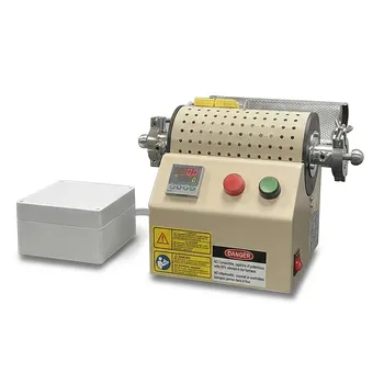
- Chemical Vapor Deposition CVD System Slide PECVD Tube Furnace with Liquid Gasifier PECVD Machine
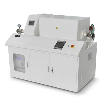
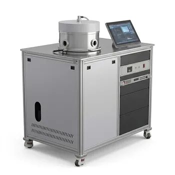
- Radio Frequency Plasma Enhanced Chemical Vapor Deposition RF PECVD System for Laboratory and Industrial Thin Film Growth
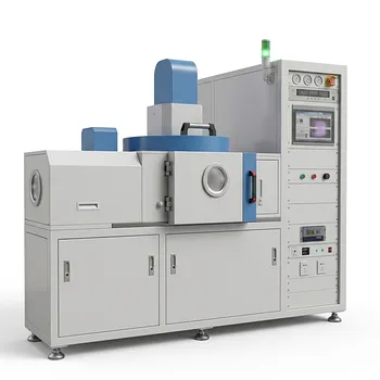
- Inclined Rotary Plasma Enhanced Chemical Vapor Deposition PECVD System for Thin Film Deposition and Nanomaterial Synthesis
- 1200C Max Compact Auto-Sliding PECVD Furnace with 2 Inch Tube and Vacuum Pump
- 1200C Dual Sliding Tube Furnace with Dual Tubes and Flanges for PECVD Processes
People Also Ask
- What are the advantages of PECVD systems for nano flame retardant films? Protect Heat-Sensitive Polymers with Precision
- How does a sliding rail design benefit the CVD process within a furnace ventilation hood? Enhance Control & Quenching
- What is the role of CVD/PECVD systems in the research of optoelectronic materials and functional coatings? Expert Guide
- How does PECVD differ from conventional thermal CVD? Key Advantages of Low-Temperature Deposition for R&D
- What role do by-product desorption and evacuation play in CVD film quality? Key Factors for High-Purity Films

Tech Team · ThermUnits
Last updated on Jun 03, 2026
Related Products
Chemical Vapor Deposition CVD System Slide PECVD Tube Furnace with Liquid Gasifier PECVD Machine
Radio Frequency Plasma Enhanced Chemical Vapor Deposition RF PECVD System for Laboratory and Industrial Thin Film Growth
Inclined Rotary Plasma Enhanced Chemical Vapor Deposition PECVD System for Thin Film Deposition and Nanomaterial Synthesis
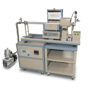
1200C Max Compact Auto-Sliding PECVD Furnace with 2 Inch Tube and Vacuum Pump
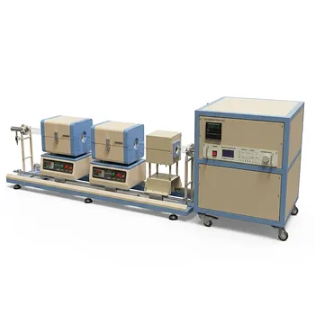
1200C Dual Sliding Tube Furnace with Dual Tubes and Flanges for PECVD Processes
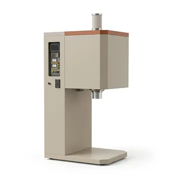
Vertical Openable Tube Furnace 0-1700c High Temperature Laboratory System for CVD and Vacuum Heat Treatment
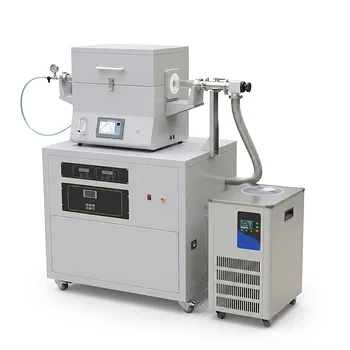
Split Chamber CVD Tube Furnace with Vacuum Station Chemical Vapor Deposition System Machine
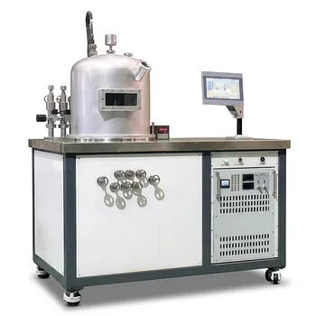
HFCVD Machine System for Nano Diamond Coating on Drawing Dies and Industrial Tools
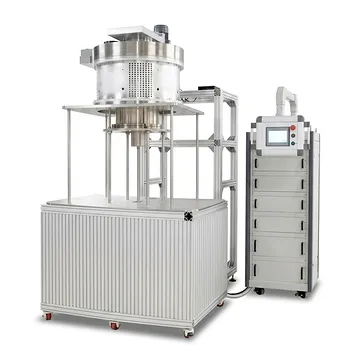
915MHz MPCVD Diamond Machine Microwave Plasma Chemical Vapor Deposition System Reactor
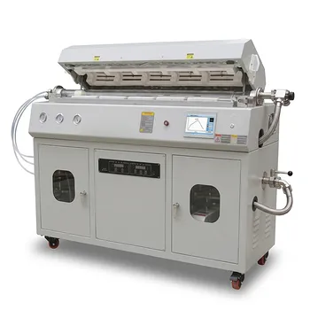
Multi Heating Zones CVD Tube Furnace System for Precision Chemical Vapor Deposition and Advanced Material Synthesis
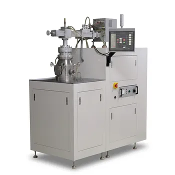
Cylindrical Resonator MPCVD Machine System for Microwave Plasma Chemical Vapor Deposition and Lab Diamond Growth
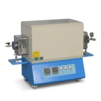
High Temperature Dual Zone Vacuum Tube Furnace for Material Research and CVD Processing
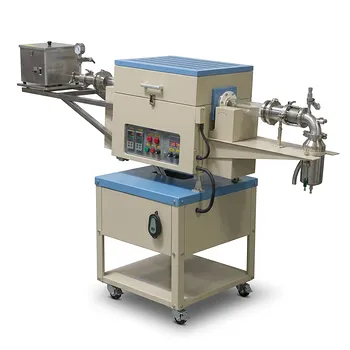
Two Zone Rotary CVD Furnace with Automatic Feeding and Receiving System for Powder Processing
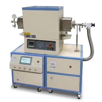
High Temperature 1700C Tube Furnace with High Vacuum Turbomolecular Pump System and Multi Channel Mass Flow Controller Gas Mixer
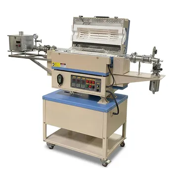
5 Inch Rotary Tube Furnace with Automatic Feeding and Receiving System 1200C Three Zone CVD Powder Processing
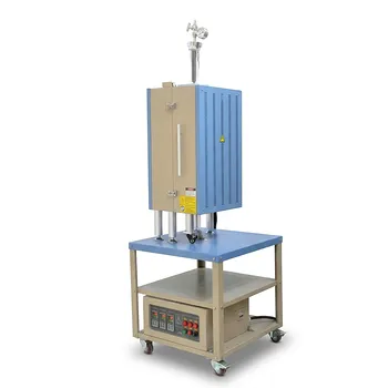
1200C Three Zone Vertical Tube Furnace with 2 Inch Quartz Tube and Vacuum Flanges
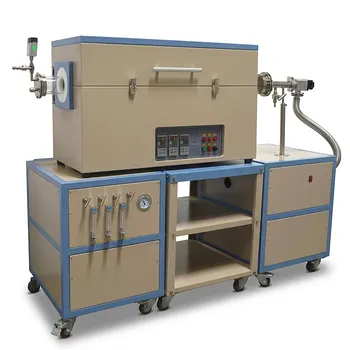
Three Zone Quartz Tube Furnace with 3 Channel Gas Mixer Vacuum Pump and Anti Corrosive Vacuum Gauge
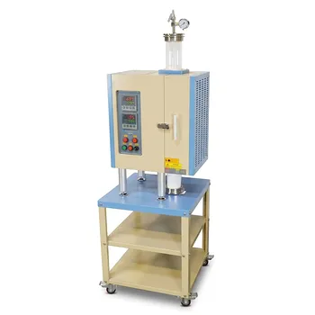
1100°C Dual Zone Split Vertical Tube Furnace with 4 Inch Quartz Tube and Vacuum Sealing Flanges
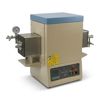
High Temperature 1700C Benchtop Tube Furnace with 5 Inch Heating Zone High Purity Alumina Tube and Vacuum Sealing Flanges