What is the role of CVD/PECVD systems in the research of optoelectronic materials and functional coatings? Expert Guide
Updated 3 weeks ago
CVD and PECVD systems serve as the foundational technology for depositing high-quality, nanometer-scale thin films with extreme precision. By regulating gaseous precursors and energy fields, these systems enable researchers to grow uniform coatings that are essential for semiconductor devices, optical filters, and advanced two-dimensional materials.
CVD and PECVD systems provide the atomic-level control necessary to engineer material properties like refractive index and hardness. Their ability to synthesize dense, pinhole-free films across large areas makes them indispensable for developing next-generation optoelectronics and protective functional coatings.
Precision Control of Thin Film Growth
Molecular-Level Chemical Synthesis
CVD and PECVD systems facilitate chemical reactions of gaseous precursors directly on a substrate surface. This process allows for controlled molecular-level reactions, resulting in films that range from a few atomic layers to several micrometers in thickness.
Uniformity Across Large Areas
These systems ensure material quality by precisely regulating gas-phase composition, flow rates, and reaction pressure. This high level of control ensures that thin films maintain uniform thickness and density even when applied to large-scale substrates.
Regulating the Reaction Environment
Researchers use these systems to fine-tune the temperature field and vacuum levels within the reaction chamber. By mastering these variables, it is possible to achieve high-quality ultrathin films with specific electronic or mechanical characteristics.
The Strategic Advantage of Plasma Enhancement (PECVD)
Lowering Thermal Requirements
Traditional CVD often requires high temperatures to trigger chemical reactions, which can damage sensitive materials. PECVD introduces plasma to provide the necessary activation energy, allowing high-quality film growth at significantly lower substrate temperatures.
Protecting Heat-Sensitive Substrates
The low-temperature nature of PECVD is vital for research involving polymers or specialized glass. This capability prevents thermal distortion or melting while still achieving the desired coating performance.
Enhanced Film Density and Adhesion
The energy provided by the plasma environment typically results in films that are denser and more adherent than those produced by standard thermal methods. These properties are critical for materials that must withstand environmental stress or mechanical wear.
Optimization of Optoelectronic and Functional Properties
Refractive Index Tuning
In optoelectronic research, the ability to manipulate light is paramount. PECVD allows for precise refractive-index tuning, enabling the creation of complex broadband anti-reflection coatings and high-reflectivity stacks.
Achieving Optical Clarity
Because PECVD processes are highly controlled, they produce pinhole-free films that maintain high transparency. This is essential for optical sensors and display technologies where any defect can scatter light and degrade performance.
Superior Environmental Protection
Functional coatings produced via these methods offer exceptional mechanical durability and chemical resistance. Compared to traditional evaporated coatings, CVD-derived films provide a more robust barrier against moisture and oxidation.
Understanding the Trade-offs and Limitations
Complexity of Precursor Chemistry
One significant challenge is the management of precursor gases, which can be toxic, flammable, or highly reactive. This requires sophisticated gas delivery systems and rigorous safety protocols, increasing the complexity of the research setup.
Equipment and Operational Costs
CVD and PECVD systems represent a high capital investment compared to simpler deposition methods like spin-coating. The need for vacuum pumps, RF generators, and precise mass flow controllers leads to higher maintenance and operational costs.
Stoichiometry Control
While these systems offer high precision, maintaining the exact chemical ratio (stoichiometry) of complex multi-element films can be difficult. Minor fluctuations in gas flow or plasma power can lead to unintended changes in the material's functional properties.
How to Apply These Systems to Your Research
Making the Right Choice for Your Goal
To maximize the utility of CVD or PECVD in your project, consider the specific requirements of your substrate and the intended application of the coating.
- If your primary focus is heat-sensitive substrates: Utilize PECVD to ensure high-quality film deposition without risking thermal damage to your base material.
- If your primary focus is maximum film purity and crystallinity: Opt for high-temperature thermal CVD, which typically allows for better atomic arrangement and fewer impurities in the crystal lattice.
- If your primary focus is optical interference coatings: Leverage PECVD for its superior ability to tune refractive indices and create dense, multilayered stacks with nanometer precision.
- If your primary focus is extreme mechanical hardness: Focus on CVD processes that emphasize high-density growth and strong interfacial adhesion for protective functional coatings.
By matching the specific capabilities of CVD and PECVD to your material requirements, you can achieve the precision and performance necessary for cutting-edge optoelectronic and functional coating research.
Summary Table:
| System Type | Activation Energy | Substrate Temperature | Key Advantage |
|---|---|---|---|
| Thermal CVD | Heat | High | Exceptional film purity and crystallinity |
| PECVD | Plasma | Low | Protects heat-sensitive substrates like polymers |
| CVD/PECVD | Both | Variable | Precise refractive index tuning & uniformity |
Elevate Your Thin-Film Research with THERMUNITS
As a leading manufacturer of high-temperature laboratory equipment for material science and industrial R&D, THERMUNITS provides state-of-the-art thermal processing solutions designed to meet the rigorous demands of optoelectronic and functional coating research.
Our comprehensive range of high-performance equipment includes:
- CVD/PECVD Systems for nanometer-scale thin film growth.
- Muffle, Vacuum, Atmosphere, Tube, and Rotary Furnaces.
- Hot Press Furnaces, Dental Furnaces, and Electric Rotary Kilns.
- Vacuum Induction Melting (VIM) Furnaces and premium Thermal Elements.
Whether you are engineering next-generation semiconductors or developing advanced optical filters, our expert team is ready to help you optimize your laboratory processes. Contact us today to discover how our advanced heat treatment equipment can drive your innovation forward.
References
- Yulian He, Zhiyong Han. Preparation of the Amorphous NiCoP Nanosheet Array on Carbon Cloth for High‐Performance Solid‐State Hybrid Supercapacitor. DOI: 10.1002/slct.202304554
Mentioned Products
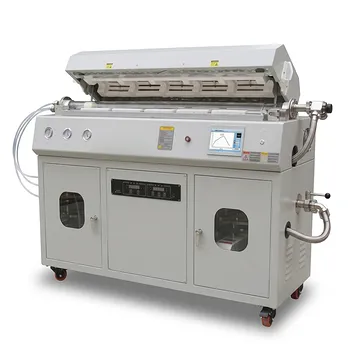
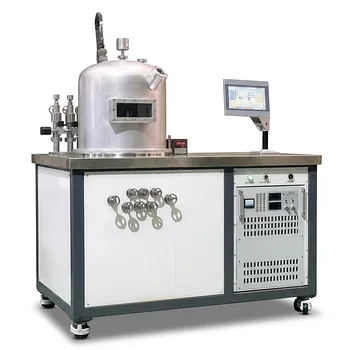
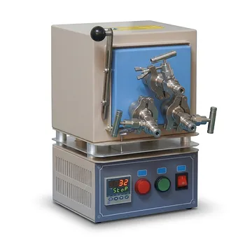
- Radio Frequency Plasma Enhanced Chemical Vapor Deposition RF PECVD System for Laboratory and Industrial Thin Film Growth
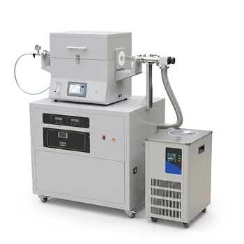
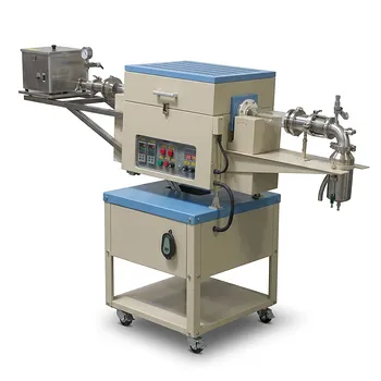
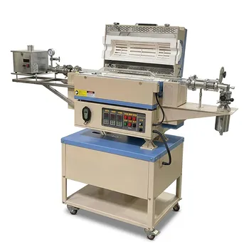
- Chemical Vapor Deposition CVD System Slide PECVD Tube Furnace with Liquid Gasifier PECVD Machine
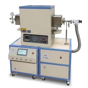
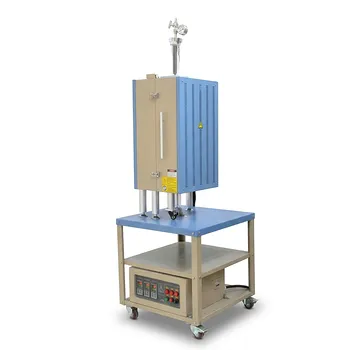
- Inclined Rotary Plasma Enhanced Chemical Vapor Deposition PECVD System for Thin Film Deposition and Nanomaterial Synthesis
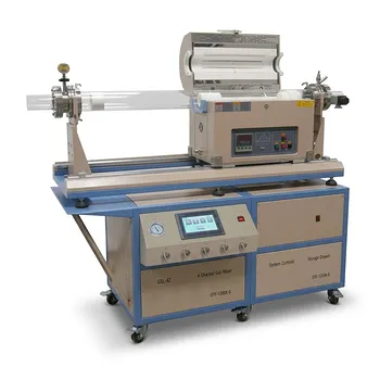
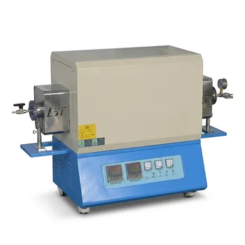
- 1200C Max Compact Auto-Sliding PECVD Furnace with 2 Inch Tube and Vacuum Pump
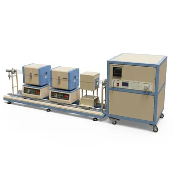
- Versatile Chemical Vapor Deposition Tube Furnace System for Advanced Material Research and Industrial Coating Processes
People Also Ask
- What are the technical advantages of the electrodeless plasma design in MPCVD systems? Purity & Precision in Synthesis
- What technical parameters are critical for optimizing the growth of single-crystal diamonds in MPCVD systems? Expert Guide
- How does the versatility of gas compatibility in MPCVD systems compare to filament-based CVD methods? Purity & Doping.
- How do Chemical Vapor Deposition (CVD) coatings enhance industrial tools? Boost Tool Life and Wear Resistance
- What are the specific advantages of using PECVD compared to thermal CVD? Low-Temp Solutions for Thin-Film Growth
Tech Team · ThermUnits
Last updated on Jun 02, 2026
Related Products
Radio Frequency Plasma Enhanced Chemical Vapor Deposition RF PECVD System for Laboratory and Industrial Thin Film Growth
Chemical Vapor Deposition CVD System Slide PECVD Tube Furnace with Liquid Gasifier PECVD Machine
Inclined Rotary Plasma Enhanced Chemical Vapor Deposition PECVD System for Thin Film Deposition and Nanomaterial Synthesis
1200C Max Compact Auto-Sliding PECVD Furnace with 2 Inch Tube and Vacuum Pump
Versatile Chemical Vapor Deposition Tube Furnace System for Advanced Material Research and Industrial Coating Processes
915MHz MPCVD Diamond Machine Microwave Plasma Chemical Vapor Deposition System Reactor
Cylindrical Resonator MPCVD Machine System for Microwave Plasma Chemical Vapor Deposition and Lab Diamond Growth
Multi Heating Zones CVD Tube Furnace System for Precision Chemical Vapor Deposition and Advanced Material Synthesis
1200C Dual Sliding Tube Furnace with Dual Tubes and Flanges for PECVD Processes
Split Chamber CVD Tube Furnace with Vacuum Station Chemical Vapor Deposition System Machine
Vertical Openable Tube Furnace 0-1700c High Temperature Laboratory System for CVD and Vacuum Heat Treatment
HFCVD Machine System for Nano Diamond Coating on Drawing Dies and Industrial Tools
Two Zone Rotary CVD Furnace with Automatic Feeding and Receiving System for Powder Processing
High Temperature 1700C Tube Furnace with High Vacuum Turbomolecular Pump System and Multi Channel Mass Flow Controller Gas Mixer
Dual Tube 100mm 80mm CVD Sliding Furnace with 4 Channel Gas Mixing and Vacuum System
Triple Tube Compact Hybrid Muffle Furnace 1000C High Vacuum Thermal Processing System
1200C Three Zone Vertical Tube Furnace with 2 Inch Quartz Tube and Vacuum Flanges
5 Inch Rotary Tube Furnace with Automatic Feeding and Receiving System 1200C Three Zone CVD Powder Processing
High Temperature Dual Zone Vacuum Tube Furnace for Material Research and CVD Processing