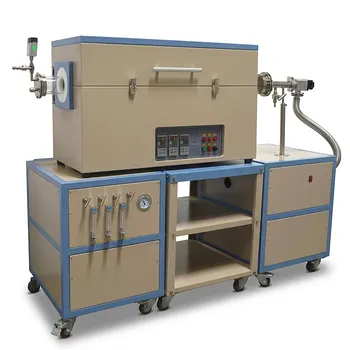
What is the core function of a CVD system in FG-FET fabrication? High-Quality Graphene Synthesis for Research
Updated 3 months ago
The core function of a Chemical Vapor Deposition (CVD) system in FG-FET fabrication is the synthesis of high-quality, large-area, single-layer graphene films. By precisely regulating the thermal decomposition of carbon-containing precursors—typically methane—the system facilitates the growth of a uniform carbon lattice on metal substrates. This process provides the essential, low-defect electrical base required to study complex microscopic electronic interactions, such as those between graphene and iron nanosheets.
Core Takeaway: A CVD system acts as a precision synthesis environment that transforms gaseous carbon precursors into a continuous, single-crystal graphene lattice. This high-quality material is the foundational component for field-effect transistors, ensuring that experimental data reflects true mechanistic interactions rather than artifacts from material defects.
The Synthesis of High-Quality Graphene
Catalytic Cracking and Deposition
The CVD system functions by inducing the catalytic decomposition of carbon-rich gases, such as methane, at high temperatures. These carbon atoms then deposit onto a metallic substrate—often copper foil or nickel foam—to form a continuous film.
Formation of the sp2-Hybridized Lattice
To function as an effective transistor channel, the carbon must form a uniform sp2-hybridized lattice. The CVD environment ensures the growth of a single-layer structure that facilitates efficient electron transport pathways, which is critical for high-performance device characteristics.
Precision Control of Process Variables
The system maintains a controlled thermal environment and atmospheric composition by regulating gas flow rates (methane, hydrogen, and argon) and pressure. This accuracy allows researchers to dictate the number of graphene layers and the orientation of the crystals.
Creating a Platform for Mechanistic Research
Minimizing Lattice Defects
For mechanistic research, particularly when studying interactions with materials like iron nanosheets, the graphene must have minimal lattice defects. The CVD process reduces structural irregularities that would otherwise scatter carriers and obscure the underlying physics being studied.
Enabling Large-Area Uniformity
Unlike mechanical exfoliation, CVD produces large-area, continuous films that are necessary for fabricating multiple devices with consistent properties. This uniformity is vital for ensuring that research findings are reproducible across different transistor samples.
High Carrier Mobility and Transparency
The high crystalline quality achieved through CVD results in films with high carrier mobility and optical transparency. These properties are essential for field-effect transistors where the collection efficiency of photogenerated carriers or the sensitivity to external gates is the primary focus.
Understanding the Trade-offs and Challenges
Substrate Transfer Complications
While CVD grows graphene on metal catalysts, the material must eventually be transferred to an insulating substrate (like silicon dioxide) to function in a FET. This transfer process can introduce polymers, residues, or mechanical tears that may degrade the electronic properties of the original film.
Temperature and Energy Constraints
CVD systems often require temperatures up to 900°C or higher to effectively crack carbon precursors. These extreme thermal requirements can limit the types of substrates used during initial growth and increase the energy intensity of the fabrication process.
Vacuum vs. Atmospheric Pressure
Researchers must choose between High-Vacuum (HV) and Atmospheric Pressure (AP) CVD systems. While HV systems offer better control over impurities and uniform growth, AP systems can sometimes offer faster growth rates and simpler hardware requirements at the cost of potential contamination.
How to Apply This to Your Project
Recommendations for System Configuration
The optimal use of a CVD system depends on the specific goals of your electronic interaction studies.
- If your primary focus is fundamental electronic transport: Prioritize a high-vacuum CVD setup to ensure the highest crystalline quality and lowest defect density for your graphene channel.
- If your primary focus is device scaling and throughput: Utilize atmospheric pressure CVD (APCVD) on copper foils to produce large-area films quickly for multi-device testing.
- If your primary focus is complex 3D architectures: Focus on using nickel foam templates within the CVD system to grow graphene that follows the geometry of the catalyst for specialized sensor applications.
By mastering the precise regulation of gas ratios and temperature within the CVD system, you establish the material integrity necessary for definitive mechanistic research in graphene electronics.
Summary Table:
| Process Step | Core Function | Impact on FG-FET |
|---|---|---|
| Precursor Cracking | Catalytic decomposition of CH4 | Pure carbon source for deposition |
| Lattice Formation | sp2-hybridized layer growth | Ensures high carrier mobility |
| Environment Control | Gas flow & pressure regulation | Uniform, single-layer crystal structure |
| Substrate Selection | Metallic catalyst (Cu/Ni) support | Facilitates large-area film consistency |
Elevate Your Material Research with THERMUNITS
As a leading manufacturer of high-temperature laboratory equipment, THERMUNITS provides the precision tools required for advanced graphene and 2D material synthesis. Our high-performance CVD and PECVD systems are engineered to deliver the uniform, low-defect films essential for Graphene Field-Effect Transistors (FG-FET) and mechanistic electronic research.
Beyond CVD, we offer a comprehensive suite of thermal processing solutions for material science and industrial R&D, including:
- Muffle, Vacuum, and Tube Furnaces for precise laboratory heat treatment.
- Atmosphere, Rotary, and Hot Press Furnaces tailored to complex material needs.
- Dental Furnaces, Electric Rotary Kilns, and Vacuum Induction Melting (VIM) systems.
- Thermal Elements and specialized laboratory components.
Partner with THERMUNITS to achieve superior material integrity and reproducible experimental results.
Contact our experts today to find your heat treatment solution
References
- Kaili Zhang, Xiaoxiao Huang. Tracking Regulatory Mechanism of Trace Fe on Graphene Electromagnetic Wave Absorption. DOI: 10.1007/s40820-023-01280-6
Mentioned Products
- Chemical Vapor Deposition CVD System Slide PECVD Tube Furnace with Liquid Gasifier PECVD Machine
- Versatile Chemical Vapor Deposition Tube Furnace System for Advanced Material Research and Industrial Coating Processes
- Radio Frequency Plasma Enhanced Chemical Vapor Deposition RF PECVD System for Laboratory and Industrial Thin Film Growth
- Inclined Rotary Plasma Enhanced Chemical Vapor Deposition PECVD System for Thin Film Deposition and Nanomaterial Synthesis
- 915MHz MPCVD Diamond Machine Microwave Plasma Chemical Vapor Deposition System Reactor
People Also Ask
- What are the advantages of PECVD systems for nano flame retardant films? Protect Heat-Sensitive Polymers with Precision
- How does a sliding rail design benefit the CVD process within a furnace ventilation hood? Enhance Control & Quenching
- What is the role of CVD/PECVD systems in the research of optoelectronic materials and functional coatings? Expert Guide
- How does PECVD differ from conventional thermal CVD? Key Advantages of Low-Temperature Deposition for R&D
- What role do by-product desorption and evacuation play in CVD film quality? Key Factors for High-Purity Films

Tech Team · ThermUnits
Last updated on Jun 02, 2026
Related Products
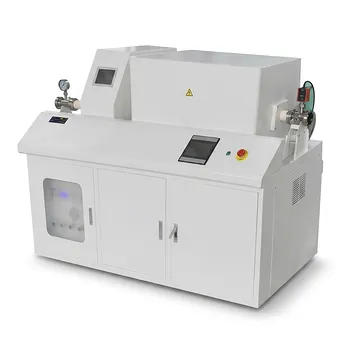
Chemical Vapor Deposition CVD System Slide PECVD Tube Furnace with Liquid Gasifier PECVD Machine
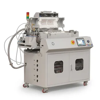
Versatile Chemical Vapor Deposition Tube Furnace System for Advanced Material Research and Industrial Coating Processes
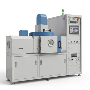
Radio Frequency Plasma Enhanced Chemical Vapor Deposition RF PECVD System for Laboratory and Industrial Thin Film Growth
Inclined Rotary Plasma Enhanced Chemical Vapor Deposition PECVD System for Thin Film Deposition and Nanomaterial Synthesis
915MHz MPCVD Diamond Machine Microwave Plasma Chemical Vapor Deposition System Reactor
Cylindrical Resonator MPCVD Machine System for Microwave Plasma Chemical Vapor Deposition and Lab Diamond Growth
Multi Heating Zones CVD Tube Furnace System for Precision Chemical Vapor Deposition and Advanced Material Synthesis
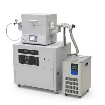
Split Chamber CVD Tube Furnace with Vacuum Station Chemical Vapor Deposition System Machine
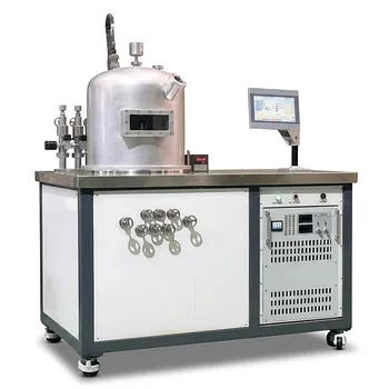
HFCVD Machine System for Nano Diamond Coating on Drawing Dies and Industrial Tools
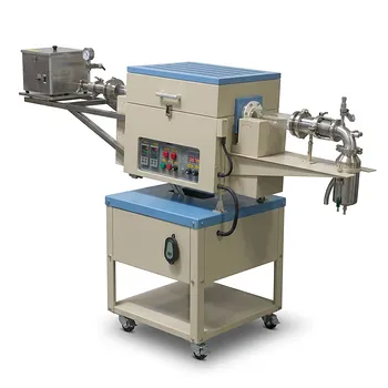
Two Zone Rotary CVD Furnace with Automatic Feeding and Receiving System for Powder Processing
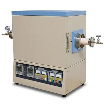
High Temperature 1700C Dual Zone Tube Furnace for Material Science and Industrial Chemical Vapor Deposition Research
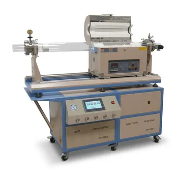
Dual Tube 100mm 80mm CVD Sliding Furnace with 4 Channel Gas Mixing and Vacuum System
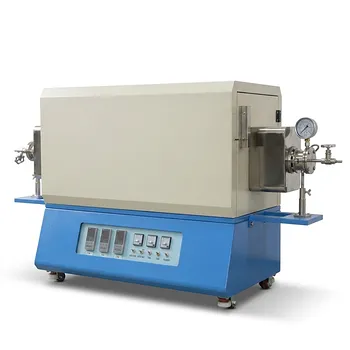
Three Temperature Zone High Temperature Vacuum Tube Furnace for CVD and Material Sintering
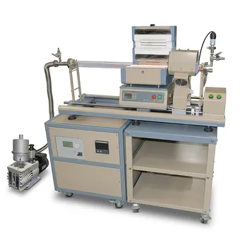
1200C Max Compact Auto-Sliding PECVD Furnace with 2 Inch Tube and Vacuum Pump
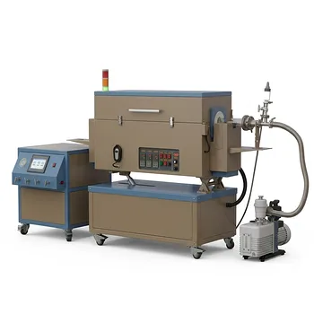
5 Inch Three Zone Rotary Tube Furnace with Integrated Gas Delivery System and 1200C Capability for Advanced Material CVD Processing
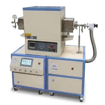
High Temperature 1700C Tube Furnace with High Vacuum Turbomolecular Pump System and Multi Channel Mass Flow Controller Gas Mixer
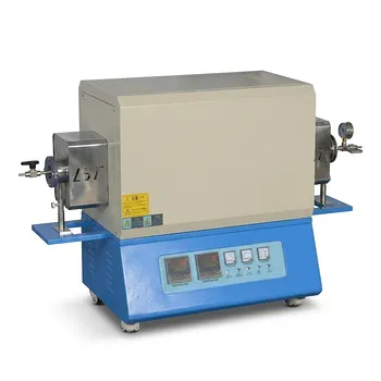
High Temperature Dual Zone Vacuum Tube Furnace for Material Research and CVD Processing
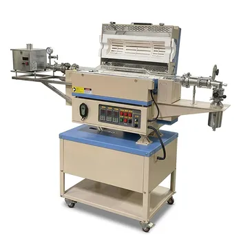
5 Inch Rotary Tube Furnace with Automatic Feeding and Receiving System 1200C Three Zone CVD Powder Processing
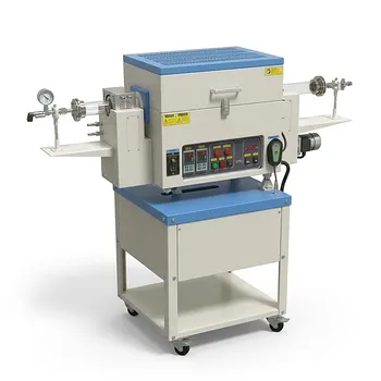
4 Inch Two Zone Rotary CVD Tube Furnace for High Temperature Battery Material Synthesis and Advanced Material Calcination