What is the primary function of a CVD system in the synthesis of Bi2O2Se thin films? Master High-Quality Crystal Growth
Updated 3 months ago
The primary function of a Chemical Vapor Deposition (CVD) system in the synthesis of $Bi_2O_2Se$ thin films is to provide a strictly controlled environment for high-quality crystal growth. By precisely regulating precursor flow rates, reaction temperatures, and pressure levels, the system facilitates the production of large-area, single-crystal films. This level of control is essential for achieving adjustable thicknesses, which are required for advanced applications like subband engineering and observing the Quantum Hall Effect.
The CVD system acts as a precision reactor that transforms gaseous precursors into solid thin films. Its ability to maintain thermodynamic stability allows for the growth of highly ordered $Bi_2O_2Se$ lattices with the uniformity necessary for quantum electronic applications.
Precise Regulation of the Growth Environment
Control of Precursor Vaporization and Flow
A CVD system manages the delivery of chemical precursors to the substrate by regulating carrier gas flow and vaporization temperatures. This ensures a consistent supply of reacting atoms, such as Bismuth and Selenium, which is critical for maintaining the stoichiometry of the $Bi_2O_2Se$ crystal lattice.
Thermodynamic Stability and Reaction Kinetics
The system provides a stable thermal and flow field, which is vital for gas-phase chemical reactions to occur predictably. By managing the reaction chamber's vacuum level and temperature, the CVD process ensures that precursors undergo controlled decomposition and deposition on the substrate surface.
Dual-Zone Thermal Management
In many synthesis setups, the CVD furnace utilizes multiple heating zones to independently control the sublimation of precursors and the epitaxial growth on the substrate. This separation allows researchers to optimize the vapor pressure of volatile materials without overheating the growing film.
Achieving Structural Excellence in $Bi_2O_2Se$
Scalability and Large-Area Uniformity
One of the most significant advantages of CVD is its ability to synthesize films over large surface areas while maintaining high quality. Unlike manual exfoliation, CVD provides a scalable pathway for creating $Bi_2O_2Se$ semiconductor films that are suitable for industrial-scale electronic devices.
Atomic-Scale Thickness Control
The CVD system allows for the precise adjustment of film thickness, which is a key requirement for "subband engineering." By manipulating the growth time and precursor concentration, researchers can produce films thin enough to observe discrete energy levels and quantum transport phenomena.
Formation of Single-Crystal Structures
The controlled environment minimizes defects and grain boundaries within the $Bi_2O_2Se$ layer. High-quality single crystals are essential for maximizing carrier mobility and ensuring that the material performs reliably in high-speed transistors and sensors.
Understanding the Trade-offs
Complexity of Parameter Optimization
The primary challenge of using a CVD system is the extreme sensitivity of the results to minor fluctuations in temperature or pressure. Even a slight deviation in the carrier gas flow rate can lead to non-uniform film thickness or the formation of unwanted phases.
Precursor and Equipment Costs
Maintaining a high-vacuum, high-temperature environment requires specialized equipment and high-purity precursors. While the process is scalable, the initial setup costs and the maintenance of a contamination-free reaction chamber can be significant.
Substrate Compatibility
The quality of $Bi_2O_2Se$ growth is highly dependent on the choice of substrate and its lattice match with the thin film. CVD processes must be carefully tailored to the specific thermal expansion and surface chemistry of the substrate to prevent cracking or poor adhesion.
Making the Right Choice for Your Goal
When planning the synthesis of $Bi_2O_2Se$ thin films, your specific research or production requirements will dictate your approach to the CVD process.
- If your primary focus is observing quantum phenomena: Prioritize a CVD system with high-precision pressure controllers to achieve the ultra-thin, uniform layers required for subband engineering.
- If your primary focus is industrial device scaling: Focus on optimizing the gas flow dynamics and substrate size within the CVD chamber to ensure large-area uniformity and high throughput.
- If your primary focus is material purity: Utilize a dual-zone furnace setup to independently regulate precursor sublimation, reducing the risk of incomplete reactions or contamination.
The CVD system remains the definitive tool for transforming $Bi_2O_2Se$ from a laboratory curiosity into a high-performance electronic material through its unmatched precision and scalability.
Summary Table:
| Key Function | Impact on Bi2O2Se Synthesis | Critical Parameters |
|---|---|---|
| Environment Control | Ensures high-quality, single-crystal growth | Vacuum levels & Temperature |
| Precursor Regulation | Maintains stoichiometric crystal lattice | Flow rate & Vaporization temp |
| Thermal Management | Independent sublimation & epitaxial growth | Dual-zone heating profiles |
| Thickness Precision | Enables subband engineering for quantum effects | Growth time & concentration |
| Scalability | Facilitates large-area, industrial production | Gas-phase flow dynamics |
Elevate Your Material Research with THERMUNITS
Are you looking to achieve atomic-scale precision in your $Bi_2O_2Se$ synthesis? THERMUNITS is a leading manufacturer of high-temperature laboratory equipment for material science and industrial R&D. We provide the advanced thermal processing solutions you need to master complex chemical vapor deposition processes.
Our comprehensive range includes:
- High-Precision CVD/PECVD Systems for 2D material synthesis.
- Multi-Zone Tube Furnaces for independent precursor sublimation control.
- Vacuum & Atmosphere Furnaces to ensure thermodynamic stability.
- Specialized Equipment: Muffle, Rotary, Hot Press furnaces, and VIM systems.
Whether you are exploring the Quantum Hall Effect or scaling up for industrial device manufacturing, our equipment offers the reliability and uniformity required for structural excellence.
Ready to optimize your lab’s thermal processing?
Contact THERMUNITS today to find the perfect solution for your R&D needs!
References
- Oleksandr Zheliuk, U. Zeitler. Quantum Hall effect in a CVD-grown oxide. DOI: 10.1038/s41467-024-54014-6
Mentioned Products
- Chemical Vapor Deposition CVD System Slide PECVD Tube Furnace with Liquid Gasifier PECVD Machine
- Versatile Chemical Vapor Deposition Tube Furnace System for Advanced Material Research and Industrial Coating Processes
- Radio Frequency Plasma Enhanced Chemical Vapor Deposition RF PECVD System for Laboratory and Industrial Thin Film Growth
- Inclined Rotary Plasma Enhanced Chemical Vapor Deposition PECVD System for Thin Film Deposition and Nanomaterial Synthesis
- 915MHz MPCVD Diamond Machine Microwave Plasma Chemical Vapor Deposition System Reactor
People Also Ask
- What are the advantages of PECVD systems for nano flame retardant films? Protect Heat-Sensitive Polymers with Precision
- How does a sliding rail design benefit the CVD process within a furnace ventilation hood? Enhance Control & Quenching
- What is the role of CVD/PECVD systems in the research of optoelectronic materials and functional coatings? Expert Guide
- How does PECVD differ from conventional thermal CVD? Key Advantages of Low-Temperature Deposition for R&D
- What role do by-product desorption and evacuation play in CVD film quality? Key Factors for High-Purity Films

Tech Team · ThermUnits
Last updated on Jun 03, 2026
Related Products
Chemical Vapor Deposition CVD System Slide PECVD Tube Furnace with Liquid Gasifier PECVD Machine
Versatile Chemical Vapor Deposition Tube Furnace System for Advanced Material Research and Industrial Coating Processes
Radio Frequency Plasma Enhanced Chemical Vapor Deposition RF PECVD System for Laboratory and Industrial Thin Film Growth
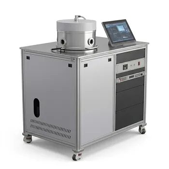
Inclined Rotary Plasma Enhanced Chemical Vapor Deposition PECVD System for Thin Film Deposition and Nanomaterial Synthesis
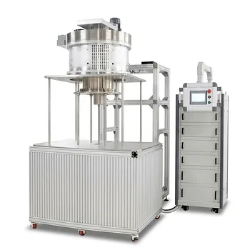
915MHz MPCVD Diamond Machine Microwave Plasma Chemical Vapor Deposition System Reactor
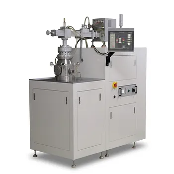
Cylindrical Resonator MPCVD Machine System for Microwave Plasma Chemical Vapor Deposition and Lab Diamond Growth
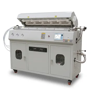
Multi Heating Zones CVD Tube Furnace System for Precision Chemical Vapor Deposition and Advanced Material Synthesis
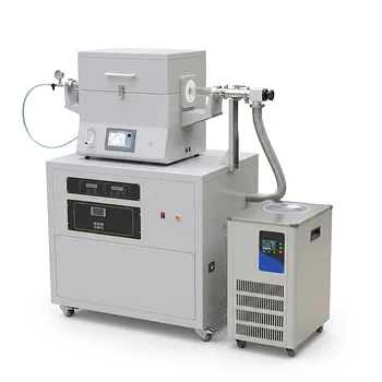
Split Chamber CVD Tube Furnace with Vacuum Station Chemical Vapor Deposition System Machine
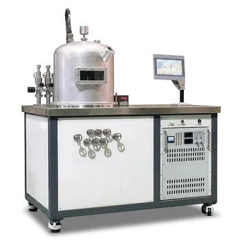
HFCVD Machine System for Nano Diamond Coating on Drawing Dies and Industrial Tools
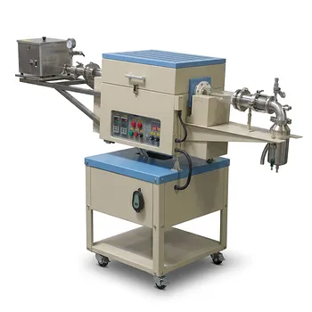
Two Zone Rotary CVD Furnace with Automatic Feeding and Receiving System for Powder Processing
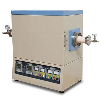
High Temperature 1700C Dual Zone Tube Furnace for Material Science and Industrial Chemical Vapor Deposition Research
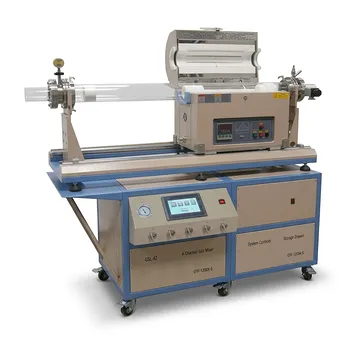
Dual Tube 100mm 80mm CVD Sliding Furnace with 4 Channel Gas Mixing and Vacuum System
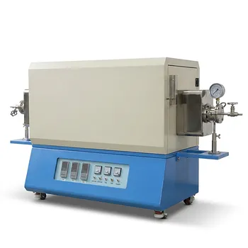
Three Temperature Zone High Temperature Vacuum Tube Furnace for CVD and Material Sintering
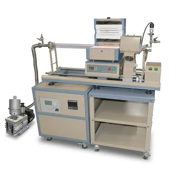
1200C Max Compact Auto-Sliding PECVD Furnace with 2 Inch Tube and Vacuum Pump
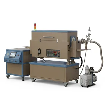
5 Inch Three Zone Rotary Tube Furnace with Integrated Gas Delivery System and 1200C Capability for Advanced Material CVD Processing
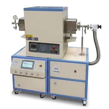
High Temperature 1700C Tube Furnace with High Vacuum Turbomolecular Pump System and Multi Channel Mass Flow Controller Gas Mixer
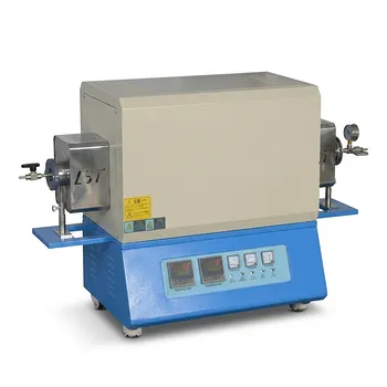
High Temperature Dual Zone Vacuum Tube Furnace for Material Research and CVD Processing
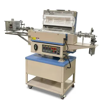
5 Inch Rotary Tube Furnace with Automatic Feeding and Receiving System 1200C Three Zone CVD Powder Processing
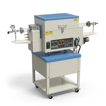
4 Inch Two Zone Rotary CVD Tube Furnace for High Temperature Battery Material Synthesis and Advanced Material Calcination