What is the role of a CVD system in graphene photodetectors? Optimize Device Sensitivity with High-Quality Graphene
Updated 3 months ago
The primary role of a Chemical Vapor Deposition (CVD) system is to synthesize high-quality, large-area monolayer graphene that serves as a transparent conductive electrode. By precisely controlling thermal environments and gas-phase reactions, the CVD system produces graphene films with the high carrier mobility and optical transparency necessary to enhance the collection efficiency of photogenerated carriers in devices like Nickel Oxide (NiO)/Silicon (Si) detectors.
Core Takeaway: A CVD system provides the strictly regulated thermal and chemical environment required to grow uniform, sp2-hybridized graphene. This process is the foundational step in ensuring the resulting photodetector achieves high charge transport efficiency without sacrificing light transmission.
The CVD Synthesis Process: Engineering the Atomic Lattice
Precision Thermal and Atmospheric Control
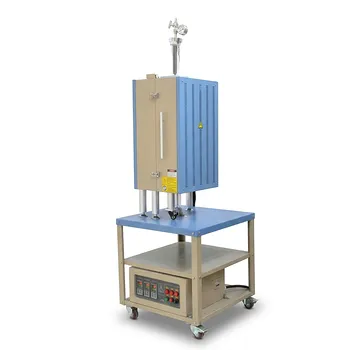
The CVD system, often utilizing a high-precision tube furnace, provides a stable high-temperature environment typically ranging from 900°C to 1050°C. This intense heat is required to facilitate the catalytic decomposition of carbon precursors, such as methane (CH4), on metal catalysts like copper foil or nickel foam.
Gas Flow and Chemical Precursors
The system accurately regulates the flow and ratio of mixed gases, specifically methane (CH4), hydrogen (H2), and argon (Ar). Methane serves as the carbon source, while hydrogen acts as a co-catalyst that helps control the grain size and morphology of the graphene, ensuring a uniform sp2-hybridized carbon lattice.
Large-Area Uniformity
For industrial applications, CVD furnaces are designed to ensure consistency across large surface areas, including 200mm wafer-level growth. This uniformity is critical for maintaining the structural integrity and atomic-level thickness of the graphene, which prevents local variations in electrical resistance or light absorption.
Impact on Photodetector Performance
Optimization of Carrier Mobility
High carrier mobility is essential for the rapid transport of electrons and holes generated by incident light. The CVD process minimizes lattice defects, creating effective electron transport pathways that significantly reduce the recombination of charge carriers.
Achieving High Optical Transparency
Because the CVD system can be tuned to produce monolayer graphene, the resulting films maintain exceptional optical transparency. This allows the maximum amount of light to reach the active layers of the photodetector (such as the silicon substrate), maximizing the device's external quantum efficiency.
Enhancing Collection Efficiency
In a NiO/Si detector architecture, the graphene produced by CVD serves as the top electrode. Its superior conductivity and contact properties allow it to efficiently "collect" photogenerated carriers, translating light signals into measurable electrical current with minimal loss.
Understanding the Trade-offs and Challenges
Substrate Transfer Complexity
While CVD grows graphene on metal catalysts like copper, the graphene must eventually be transferred to the photodetector substrate (e.g., Silicon). This transfer process can introduce mechanical strain, tears, or chemical residues that may degrade the material's ideal properties.
Temperature and Energy Demands
Operating at temperatures above 1000°C requires significant energy and specialized equipment capable of maintaining a high-vacuum environment. These requirements can increase the cost and complexity of the fabrication process compared to lower-quality solution-processed alternatives.
Precursor Purity and Contamination
The quality of the graphene is highly sensitive to the purity of the precursor gases. Even trace amounts of oxygen or other impurities during the CVD process can lead to unintended doping or defects in the carbon lattice, negatively impacting the photodetector’s noise levels.
How to Apply CVD Technology to Your Project
Making the Right Choice for Your Goal
- If your primary focus is Maximum Sensitivity: Prioritize a high-vacuum CVD system with precise H2/CH4 ratio control to ensure a defect-free lattice for the highest possible carrier mobility.
- If your primary focus is Industrial Scalability: Utilize an industrial-grade CVD furnace capable of uniform growth on 200mm wafers to ensure consistent device performance across large batches.
- If your primary focus is Device Transparency: Focus on optimizing growth parameters to ensure strictly monolayer deposition, as multi-layer graphene will increase light absorption and reduce detector efficiency.
The CVD system is the indispensable engine of graphene fabrication, transforming raw carbon gases into the high-performance transparent electrodes that define modern optoelectronics.
Summary Table:
| CVD Process Feature | Technical Specification/Parameter | Impact on Photodetector Performance |
|---|---|---|
| Thermal Control | 900°C to 1050°C Precision | Catalytic decomposition for uniform sp2-hybridized lattice |
| Gas Regulation | CH4, H2, and Ar flow control | Minimizes defects to optimize carrier mobility and transport |
| Layer Precision | Monolayer Graphene Growth | Maximizes optical transparency and external quantum efficiency |
| Scalability | Large-area/Wafer-level growth | Ensures consistent electrical resistance across large devices |
Elevate Your Material Research with THERMUNITS Precision
High-performance photodetectors demand the absolute highest quality graphene, which can only be achieved through rigorous thermal and atmospheric control. As a leading manufacturer of high-temperature laboratory equipment for material science and industrial R&D, THERMUNITS provides the advanced CVD and thermal processing solutions required for cutting-edge optoelectronics.
Whether you are focusing on graphene synthesis, thin-film deposition, or advanced semiconductor research, our comprehensive range of equipment is designed to meet your exact specifications:
- CVD/PECVD Systems for high-quality 2D material growth.
- Tube & Atmosphere Furnaces for precise chemical vapor reactions.
- Vacuum, Muffle, and Rotary Furnaces for diverse heat treatment needs.
- Advanced Solutions: Hot Press, Dental Furnaces, VIM, and high-performance Thermal Elements.
Ready to optimize your fabrication process? Contact THERMUNITS today to discuss your specific research goals and discover how our laboratory heat treatment solutions can enhance your lab's efficiency and output.
References
- Bhishma Pandit, Keun Heo. Self-Powered Broadband Photodetector Based on NiO/Si Heterojunction Incorporating Graphene Transparent Conducting Layer. DOI: 10.3390/nano14060551
Mentioned Products
- Radio Frequency Plasma Enhanced Chemical Vapor Deposition RF PECVD System for Laboratory and Industrial Thin Film Growth
- Versatile Chemical Vapor Deposition Tube Furnace System for Advanced Material Research and Industrial Coating Processes
- Chemical Vapor Deposition CVD System Slide PECVD Tube Furnace with Liquid Gasifier PECVD Machine
- Cylindrical Resonator MPCVD Machine System for Microwave Plasma Chemical Vapor Deposition and Lab Diamond Growth
- 915MHz MPCVD Diamond Machine Microwave Plasma Chemical Vapor Deposition System Reactor
People Also Ask
- What are the advantages of PECVD systems for nano flame retardant films? Protect Heat-Sensitive Polymers with Precision
- How does PECVD differ from conventional thermal CVD? Key Advantages of Low-Temperature Deposition for R&D
- What is the role of CVD/PECVD systems in the research of optoelectronic materials and functional coatings? Expert Guide
- What are the benefits of using PECVD for optical and photonic coatings? Achieve High-Precision Thin-Film Deposition
- How do RF frequency and power settings influence the characteristics of a PECVD process? Master Quality & Efficiency

Tech Team · ThermUnits
Last updated on Jun 03, 2026
Related Products
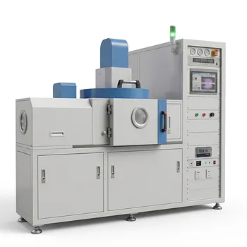
Radio Frequency Plasma Enhanced Chemical Vapor Deposition RF PECVD System for Laboratory and Industrial Thin Film Growth
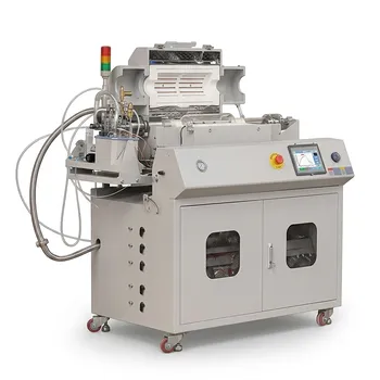
Versatile Chemical Vapor Deposition Tube Furnace System for Advanced Material Research and Industrial Coating Processes
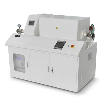
Chemical Vapor Deposition CVD System Slide PECVD Tube Furnace with Liquid Gasifier PECVD Machine
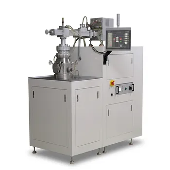
Cylindrical Resonator MPCVD Machine System for Microwave Plasma Chemical Vapor Deposition and Lab Diamond Growth
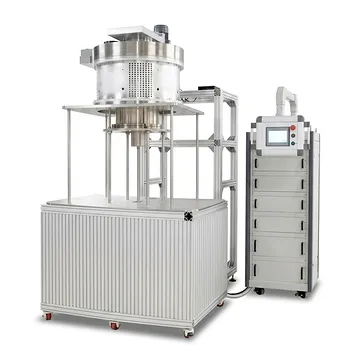
915MHz MPCVD Diamond Machine Microwave Plasma Chemical Vapor Deposition System Reactor
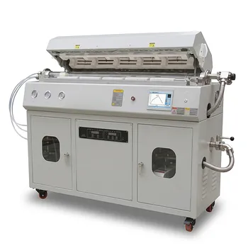
Multi Heating Zones CVD Tube Furnace System for Precision Chemical Vapor Deposition and Advanced Material Synthesis
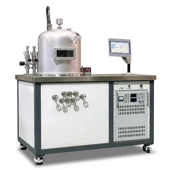
HFCVD Machine System for Nano Diamond Coating on Drawing Dies and Industrial Tools
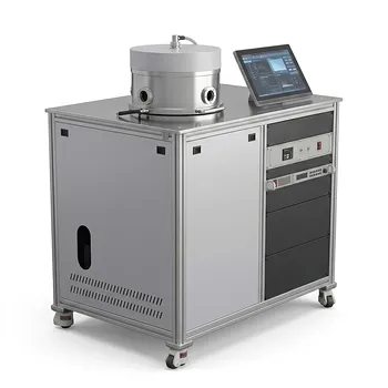
Inclined Rotary Plasma Enhanced Chemical Vapor Deposition PECVD System for Thin Film Deposition and Nanomaterial Synthesis
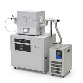
Split Chamber CVD Tube Furnace with Vacuum Station Chemical Vapor Deposition System Machine
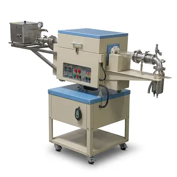
Two Zone Rotary CVD Furnace with Automatic Feeding and Receiving System for Powder Processing
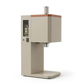
Vertical Openable Tube Furnace 0-1700c High Temperature Laboratory System for CVD and Vacuum Heat Treatment
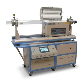
Dual Tube 100mm 80mm CVD Sliding Furnace with 4 Channel Gas Mixing and Vacuum System
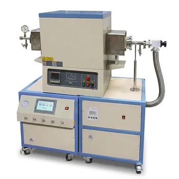
High Temperature 1700C Tube Furnace with High Vacuum Turbomolecular Pump System and Multi Channel Mass Flow Controller Gas Mixer
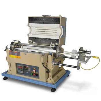
1200°C High Temperature 4 Inch Tube Furnace with Sliding Flange for CVD Systems
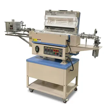
5 Inch Rotary Tube Furnace with Automatic Feeding and Receiving System 1200C Three Zone CVD Powder Processing
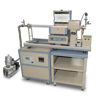
1200C Max Compact Auto-Sliding PECVD Furnace with 2 Inch Tube and Vacuum Pump
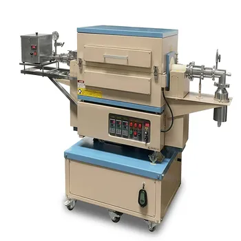
1500C 3-Zone Rotary Tube Furnace 60mm with Automatic Powder Feeding and Receiving System for Continuous Material Synthesis
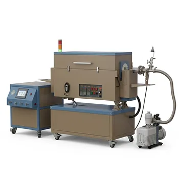
5 Inch Three Zone Rotary Tube Furnace with Integrated Gas Delivery System and 1200C Capability for Advanced Material CVD Processing
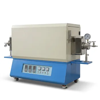
Three Temperature Zone High Temperature Vacuum Tube Furnace for CVD and Material Sintering