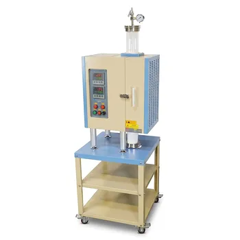
What are the benefits of using PECVD for optical and photonic coatings? Achieve High-Precision Thin-Film Deposition
Updated 5 months ago
The primary benefits of Plasma-Enhanced Chemical Vapor Deposition (PECVD) for optical coatings are its low processing temperature and its exceptional control over thin-film properties. By using plasma to drive chemical reactions rather than heat, PECVD allows for the deposition of high-quality, dense, and pinhole-free films at temperatures typically between 200°C and 400°C. This enables the creation of high-precision optical stacks—such as anti-reflection or high-reflectivity coatings—on temperature-sensitive substrates like polymers and glass without causing thermal distortion or damage.
PECVD is a transformative technology for photonics because it decouples the energy required for chemical reactions from the substrate temperature. This allows engineers to achieve high-density, precisely tuned optical films on sensitive materials that would otherwise fail under traditional thermal deposition methods.
Thermal Integrity and Substrate Versatility
Preservation of Temperature-Sensitive Materials
Standard thermal CVD requires temperatures between 600°C and 900°C, which can destroy metal interconnects or melt polymer substrates. PECVD operates at a much lower thermal budget, making it compatible with unsaturated polyester resins (UPR), aluminum, and advanced plastics used in modern optics.
Prevention of Thermal Distortion
In high-precision glass optics, even minor heat fluctuations can cause internal stresses or physical warping. Because PECVD maintains a low-temperature environment, it preserves the structural integrity and transparency of the substrate, ensuring the final optical component meets strict geometric tolerances.
Expanded Material Compatibility
This technology allows for the deposition of a diverse array of materials, including Silicon Dioxide (SiO2), Silicon Nitride (SiNx), and Silicon Oxynitride. This versatility enables designers to select the best material for specific photonic functions without being limited by the substrate's melting point.
Superior Optical and Mechanical Performance
Precise Refractive-Index Tuning
By adjusting process parameters like gas flow, pressure, and plasma power, PECVD allows for the meticulous tuning of the refractive index. This is critical for creating structural colors and complex interference filters where even a slight deviation in index can ruin the component's performance.
Atomic-Scale Thickness Control
PECVD systems provide the level of control necessary to deposit films ranging from 30 nm to 130 nm with high repeatability. This precision is essential for broadband anti-reflection (AR) coatings and high-reflectivity stacks used in laser applications and solar energy.
Enhanced Film Density and Durability
Unlike traditional evaporated coatings, PECVD films are characterized by extreme density and low porosity. This results in superior environmental protection, high mechanical hardness, and resistance to wear, which is often enhanced through controlled ion bombardment during the deposition process.
Industrial Efficiency and Specialized Applications
Excellent Step Coverage and Uniformity
PECVD excels at providing uniform coverage on complex 3D geometries, such as threads, recesses, and curved lenses. This "step coverage" ensures that the optical or protective properties are consistent across the entire surface of a component, regardless of its shape.
Hydrogen-Induced Passivation
In solar cell manufacturing, PECVD-deposited Silicon Nitride layers do more than just reduce reflection. They facilitate hydrogen-induced passivation, which improves the open-circuit voltage (Voc) and overall efficiency of the cell by neutralizing surface defects.
Wear-Resistant and Protective Coatings
Beyond light manipulation, PECVD is used to deposit Diamond-Like Carbon (DLC) and other hard coatings. These films provide low friction coefficients and high chemical resistance, protecting delicate photonic sensors from harsh operating environments.
Understanding the Trade-offs
Equipment Complexity and Cost
PECVD systems are significantly more complex and expensive to maintain than basic physical vapor deposition (PVD) or evaporation setups. The requirement for vacuum systems, RF generators, and sophisticated gas handling increases the initial capital expenditure and operational overhead.
Potential for Plasma Damage
While the low temperature is a benefit, the ion bombardment inherent in the plasma process can sometimes damage extremely sensitive surface structures. Finding the balance between high film density and surface preservation requires rigorous process optimization.
Precursor Management and Safety
The reactive gases used in PECVD, such as Silane (SiH4), are often hazardous, pyrophoric, or toxic. This necessitates advanced safety protocols, specialized exhaust scrubbing systems, and careful handling of chemical precursors, which can complicate the manufacturing workflow.
How to Apply PECVD to Your Project
When deciding whether to implement PECVD for your optical or photonic application, consider your primary performance bottleneck and substrate limitations.
- If your primary focus is coating temperature-sensitive polymers: Utilize PECVD to maintain a thermal budget below 250°C while achieving high-density dielectric layers.
- If your primary focus is high-efficiency solar or semiconductor optics: Leverage PECVD for its ability to provide both anti-reflection properties and critical surface passivation in a single step.
- If your primary focus is complex 3D lens geometries: Prioritize PECVD over evaporation to ensure uniform film thickness and optical performance across curved or recessed surfaces.
- If your primary focus is extreme environmental durability: Focus on PECVD’s ability to create pinhole-free, hard coatings like Silicon Nitride or DLC for superior mechanical protection.
By matching the specific plasma parameters to your material requirements, you can achieve a level of optical precision and structural durability that traditional coating methods cannot replicate.
Summary Table:
| Benefit | Key Feature | Industry Application |
|---|---|---|
| Low Temperature | 200°C - 400°C processing | Polymer optics & sensitive glass |
| Precision Tuning | Refractive index & thickness control | AR coatings & interference filters |
| High Film Quality | Dense, pinhole-free, & hard films | Solar cells & laser components |
| Uniform Coverage | Excellent 3D step coverage | Curved lenses & complex sensors |
Optimize Your Optical Coatings with THERMUNITS PECVD Systems
As a leading manufacturer of high-temperature laboratory equipment, THERMUNITS provides state-of-the-art thermal processing solutions tailored for material science and industrial R&D. Our comprehensive range includes specialized PECVD/CVD systems, muffle, vacuum, and tube furnaces designed to achieve the precision and durability your photonic applications demand.
From temperature-sensitive polymer substrates to high-efficiency solar optics, our heat treatment experts help you select the ideal equipment to ensure consistent, high-performance results.
Ready to elevate your lab's thin-film capabilities?
Contact THERMUNITS today to get a professional solution!
Mentioned Products
- Inclined Rotary Plasma Enhanced Chemical Vapor Deposition PECVD System for Thin Film Deposition and Nanomaterial Synthesis
- Radio Frequency Plasma Enhanced Chemical Vapor Deposition RF PECVD System for Laboratory and Industrial Thin Film Growth
- Chemical Vapor Deposition CVD System Slide PECVD Tube Furnace with Liquid Gasifier PECVD Machine
- 1200C Max Compact Auto-Sliding PECVD Furnace with 2 Inch Tube and Vacuum Pump
- Cylindrical Resonator MPCVD Machine System for Microwave Plasma Chemical Vapor Deposition and Lab Diamond Growth
People Also Ask
- What types of materials can be deposited using PECVD systems? Explore Versatile Thin-Film Coating Solutions
- How does the non-equilibrium nature of plasma facilitate low-temperature deposition in PECVD systems? Pro Tips for R&D
- How is Plasma-Enhanced Chemical Vapor Deposition (PECVD) utilized in the production of photovoltaic solar cells? Study
- How do RF frequency and power settings influence the characteristics of a PECVD process? Master Quality & Efficiency
- What are the advantages of PECVD systems for nano flame retardant films? Protect Heat-Sensitive Polymers with Precision

Tech Team · ThermUnits
Last updated on Apr 14, 2026
Related Products
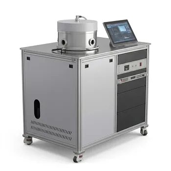
Inclined Rotary Plasma Enhanced Chemical Vapor Deposition PECVD System for Thin Film Deposition and Nanomaterial Synthesis
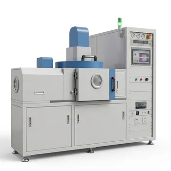
Radio Frequency Plasma Enhanced Chemical Vapor Deposition RF PECVD System for Laboratory and Industrial Thin Film Growth
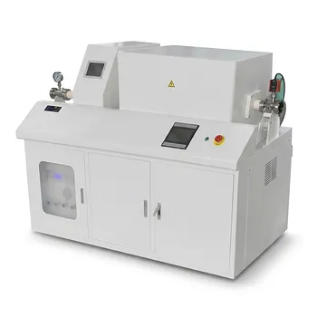
Chemical Vapor Deposition CVD System Slide PECVD Tube Furnace with Liquid Gasifier PECVD Machine
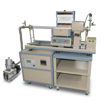
1200C Max Compact Auto-Sliding PECVD Furnace with 2 Inch Tube and Vacuum Pump
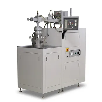
Cylindrical Resonator MPCVD Machine System for Microwave Plasma Chemical Vapor Deposition and Lab Diamond Growth
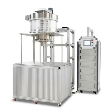
915MHz MPCVD Diamond Machine Microwave Plasma Chemical Vapor Deposition System Reactor
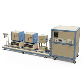
1200C Dual Sliding Tube Furnace with Dual Tubes and Flanges for PECVD Processes
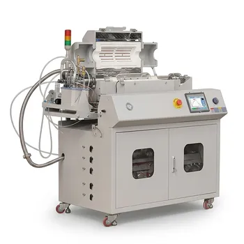
Versatile Chemical Vapor Deposition Tube Furnace System for Advanced Material Research and Industrial Coating Processes
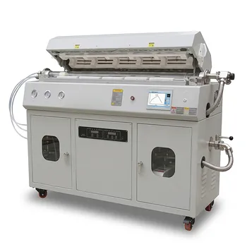
Multi Heating Zones CVD Tube Furnace System for Precision Chemical Vapor Deposition and Advanced Material Synthesis
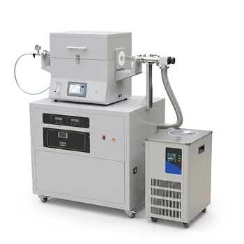
Split Chamber CVD Tube Furnace with Vacuum Station Chemical Vapor Deposition System Machine
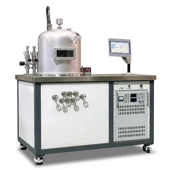
HFCVD Machine System for Nano Diamond Coating on Drawing Dies and Industrial Tools
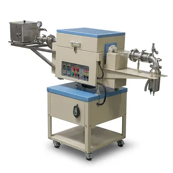
Two Zone Rotary CVD Furnace with Automatic Feeding and Receiving System for Powder Processing
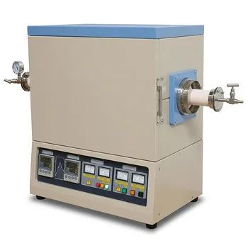
High Temperature 1700C Dual Zone Tube Furnace for Material Science and Industrial Chemical Vapor Deposition Research
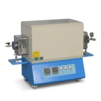
High Temperature Dual Zone Vacuum Tube Furnace for Material Research and CVD Processing
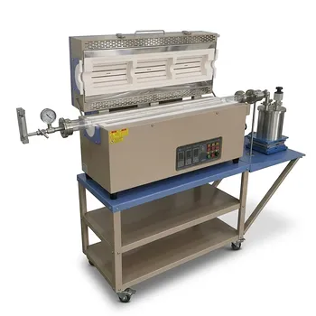
5 Inch Two Zone Rotary Tube Furnace 1100C for Powder CVD and Material Synthesis
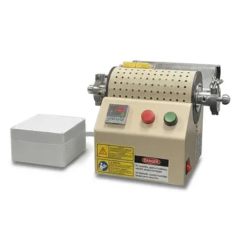
1000C Mini Tube Furnace with 20mm Quartz Tube and Vacuum Flanges for Material Science Research and Controlled Atmosphere Small Sample Processing
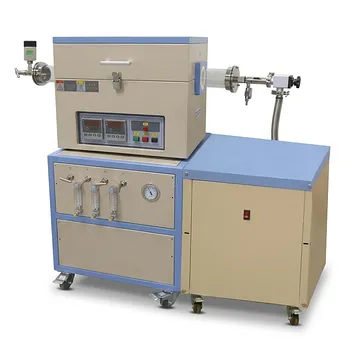
Dual Zone Quartz Tube Furnace with 80mm Diameter 1200C Max Temperature 3 Channel Gas Mixer and Vacuum Pump System
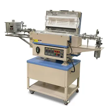
5 Inch Rotary Tube Furnace with Automatic Feeding and Receiving System 1200C Three Zone CVD Powder Processing
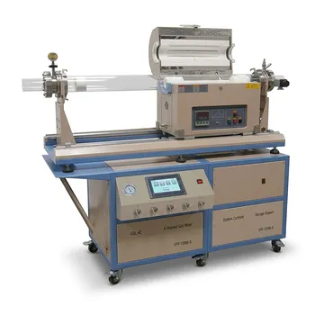
Dual Tube 100mm 80mm CVD Sliding Furnace with 4 Channel Gas Mixing and Vacuum System