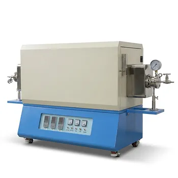
What technical advantages does PECVD offer for BEOL semiconductor processing? Precision Films at Low Temperatures
Updated 5 months ago
PECVD is a cornerstone of Back-End-of-Line (BEOL) processing due to its ability to deposit high-quality thin films at significantly reduced temperatures. By using radio frequency (RF) energy to create a plasma, the system dissociates precursor gases at temperatures between 200°C and 400°C, far below the 600°C+ required for traditional thermal CVD. This allows for the integration of temperature-sensitive materials like copper interconnects and low-k dielectrics without risking thermal degradation.
PECVD provides the essential "thermal budget" flexibility required to build complex, multi-layered interconnect structures without damaging the underlying circuitry. It bridges the gap between high-quality film requirements and the strict temperature limitations of modern semiconductor materials.
Preservation of the Thermal Budget
Lowering Activation Energy via Plasma
The primary technical advantage of PECVD is the use of an RF source to generate low-temperature plasma. This plasma excites and dissociates reaction precursors, providing the energy needed for film formation that would otherwise require high heat.
Protecting Sensitive Interconnects
In BEOL, aluminum and copper interconnects are highly susceptible to melting or unintended diffusion at high temperatures. PECVD’s operating range of 200°C to 400°C ensures these metal layers and associated polymer substrates remain structurally sound throughout the manufacturing process.
Preventing Structural Defects
By operating at lower temperatures, PECVD minimizes the risk of thermal expansion coefficient mismatch. This reduction in thermal stress prevents the warping of flexible substrates and protects delicate components like gas diffusion layers or polymer binders from degradation.
Superior Conformality and Step Coverage
Handling High-Aspect-Ratio Features
PECVD is critical for depositing films on complex 3D structures, such as Through-Silicon Vias (TSVs) and hybrid bonding insulation. It provides excellent conformal coverage, ensuring that dielectric layers are deposited uniformly even in deep, narrow trenches.
Supporting 3D Integration
As chips move toward 2.5D and 3D packaging for AI and high-performance computing, the ability to coat high-aspect-ratio features becomes paramount. PECVD enables the precise insulation required for vertical interconnects and stacked die architectures.
Avoiding the Wrap-Around Effect
Unlike diffusion furnaces used in traditional processing, industrial PECVD systems support single-sided deposition. This prevents the "wrap-around" effect, where material is unintentionally deposited on the backside of the wafer, simplifying the overall process flow.
Precision Control of Film Properties
Tunable Mechanical Stress
PECVD allows engineers to precisely tune film stress by adjusting plasma parameters such as power, pressure, and gas flow. This tunability is essential for preventing film peeling or wafer bowing in multi-layered BEOL stacks, ensuring long-term mechanical reliability.
Optical and Dielectric Customization
The process enables the fine-tuning of a film's refractive index and thickness, which is vital for applications like silicon nitride (SiNx) passivation or anti-reflection coatings. This level of control allows for the optimization of structural colors and advanced optical properties in specialized sensors or displays.
High Throughput and Material Efficiency
Industrial-grade PECVD systems offer high deposition rates and efficient precursor utilization (such as silane). This supports high-volume manufacturing (HVM) by maintaining low defect densities while increasing the speed of the production line.
Understanding the Trade-offs
Potential for Plasma-Induced Damage
While the plasma enables lower temperatures, it can also cause ion bombardment damage to the substrate surface. This requires careful calibration of the RF power to balance film density with the preservation of the underlying lattice structure.
Chemical Purity and Byproducts
Films grown via PECVD may sometimes contain higher levels of residual impurities, such as hydrogen, compared to high-temperature thermal CVD. These residuals can affect the dielectric constant or the long-term stability of the film if not properly managed through post-deposition treatments.
Equipment Complexity
The inclusion of RF generators, vacuum systems, and plasma control hardware makes PECVD systems more complex and expensive to maintain than simpler thermal systems. However, this cost is generally offset by the necessity of the low-temperature capability in modern nodes.
How to Apply This to Your Project
Recommendations Based on Goals
- If your primary focus is protecting copper or low-k dielectrics: Utilize PECVD specifically within the 250°C to 350°C range to ensure no thermal degradation occurs to your metal stack.
- If your primary focus is 3D integration or TSVs: Prioritize PECVD for its superior step coverage and ability to create uniform insulation layers in high-aspect-ratio vias.
- If your primary focus is mechanical reliability in thick stacks: Use the tunable stress capabilities of PECVD to balance the compressive or tensile forces of the film, preventing wafer warping.
- If your primary focus is optical performance (e.g., sensors): Leverage the ability to precisely control the refractive index of SiNx layers through gas flow and power adjustments.
PECVD is the definitive solution for high-performance BEOL processing, offering a sophisticated balance of low-temperature safety and high-precision material engineering.
Summary Table:
| Feature | Technical Advantage | BEOL Application Benefit |
|---|---|---|
| Low Process Temp | 200°C - 400°C range | Protects copper interconnects and low-k dielectrics from thermal damage. |
| High Conformality | Superior step coverage | Ensures uniform insulation for TSVs and high-aspect-ratio 3D structures. |
| Stress Tunability | Adjustable plasma parameters | Prevents wafer bowing and film peeling in multi-layered stacks. |
| Single-sided Deposition | No "wrap-around" effect | Simplifies processing by avoiding unintentional backside deposition. |
| Optical Control | Tunable refractive index | Optimizes SiNx passivation and anti-reflection coatings for sensors. |
Optimize Your Semiconductor R&D with THERMUNITS Expert Solutions
Are you looking to master the thermal budget of your next-generation BEOL processes? THERMUNITS is a leading manufacturer of high-performance laboratory equipment tailored for material science and industrial R&D. We specialize in advanced thermal processing solutions, including state-of-the-art CVD/PECVD systems, Vacuum, Atmosphere, and Tube furnaces designed to meet the rigorous demands of modern semiconductor fabrication.
Whether you are working on 3D integration, hybrid bonding, or advanced dielectric films, our equipment provides the precision and reliability needed for high-quality thin-film deposition. Our extensive catalog also includes Muffle, Rotary, and Hot Press furnaces, Dental Furnaces, Electric Rotary Kilns, and Vacuum Induction Melting (VIM) furnaces, ensuring a comprehensive solution for every stage of your heat treatment workflow.
Contact our technical team today to discuss your specific process requirements and discover how our expertise can accelerate your research.
👉 Get a Quote & Professional Consultation
Mentioned Products
- Inclined Rotary Plasma Enhanced Chemical Vapor Deposition PECVD System for Thin Film Deposition and Nanomaterial Synthesis
- Radio Frequency Plasma Enhanced Chemical Vapor Deposition RF PECVD System for Laboratory and Industrial Thin Film Growth
- Chemical Vapor Deposition CVD System Slide PECVD Tube Furnace with Liquid Gasifier PECVD Machine
- 1200C Max Compact Auto-Sliding PECVD Furnace with 2 Inch Tube and Vacuum Pump
- 1200C Dual Sliding Tube Furnace with Dual Tubes and Flanges for PECVD Processes
People Also Ask
- What types of materials can be deposited using PECVD systems? Explore Versatile Thin-Film Coating Solutions
- How does the non-equilibrium nature of plasma facilitate low-temperature deposition in PECVD systems? Pro Tips for R&D
- How is Plasma-Enhanced Chemical Vapor Deposition (PECVD) utilized in the production of photovoltaic solar cells? Study
- How do RF frequency and power settings influence the characteristics of a PECVD process? Master Quality & Efficiency
- What are the advantages of PECVD systems for nano flame retardant films? Protect Heat-Sensitive Polymers with Precision

Tech Team · ThermUnits
Last updated on Apr 14, 2026
Related Products
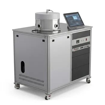
Inclined Rotary Plasma Enhanced Chemical Vapor Deposition PECVD System for Thin Film Deposition and Nanomaterial Synthesis
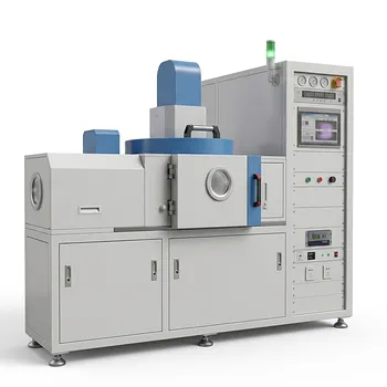
Radio Frequency Plasma Enhanced Chemical Vapor Deposition RF PECVD System for Laboratory and Industrial Thin Film Growth
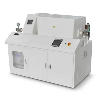
Chemical Vapor Deposition CVD System Slide PECVD Tube Furnace with Liquid Gasifier PECVD Machine
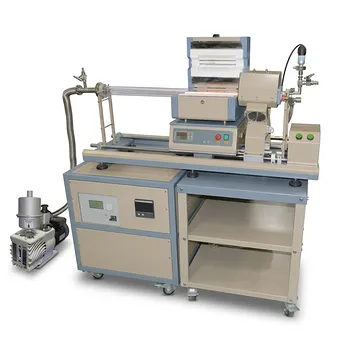
1200C Max Compact Auto-Sliding PECVD Furnace with 2 Inch Tube and Vacuum Pump
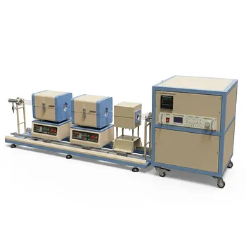
1200C Dual Sliding Tube Furnace with Dual Tubes and Flanges for PECVD Processes
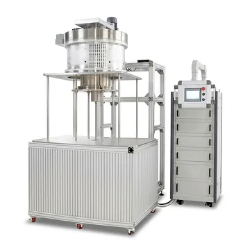
915MHz MPCVD Diamond Machine Microwave Plasma Chemical Vapor Deposition System Reactor
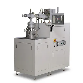
Cylindrical Resonator MPCVD Machine System for Microwave Plasma Chemical Vapor Deposition and Lab Diamond Growth
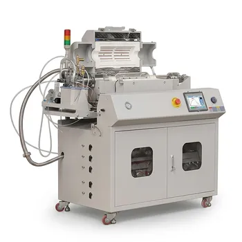
Versatile Chemical Vapor Deposition Tube Furnace System for Advanced Material Research and Industrial Coating Processes
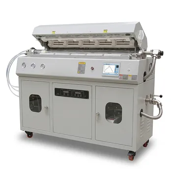
Multi Heating Zones CVD Tube Furnace System for Precision Chemical Vapor Deposition and Advanced Material Synthesis
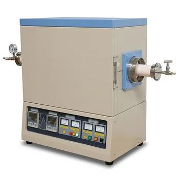
High Temperature 1700C Dual Zone Tube Furnace for Material Science and Industrial Chemical Vapor Deposition Research
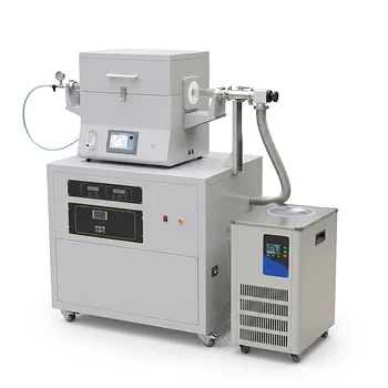
Split Chamber CVD Tube Furnace with Vacuum Station Chemical Vapor Deposition System Machine
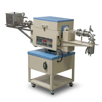
Two Zone Rotary CVD Furnace with Automatic Feeding and Receiving System for Powder Processing
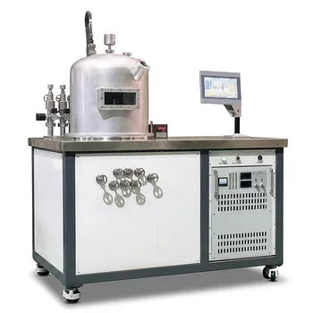
HFCVD Machine System for Nano Diamond Coating on Drawing Dies and Industrial Tools
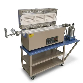
5 Inch Two Zone Rotary Tube Furnace 1100C for Powder CVD and Material Synthesis
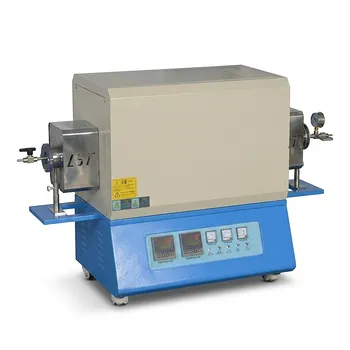
High Temperature Dual Zone Vacuum Tube Furnace for Material Research and CVD Processing
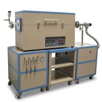
Three Zone Quartz Tube Furnace with 3 Channel Gas Mixer Vacuum Pump and Anti Corrosive Vacuum Gauge
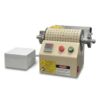
1000C Mini Tube Furnace with 20mm Quartz Tube and Vacuum Flanges for Material Science Research and Controlled Atmosphere Small Sample Processing
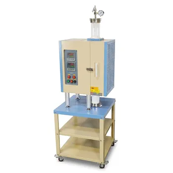
1100°C Dual Zone Split Vertical Tube Furnace with 4 Inch Quartz Tube and Vacuum Sealing Flanges