Why are carbon nanotubes synthesized via the CVD method preferred for solar cells? Boost Efficiency with High Purity
Updated 6 months ago
Chemical Vapor Deposition (CVD) is the preferred synthesis method because it produces carbon nanotubes (CNTs) with exceptional purity (exceeding 98%), structural uniformity, and tunable physical properties. These characteristics directly translate to higher carrier mobility and superior optical transparency, which are essential for maximizing the energy conversion efficiency of modern solar cells.
The primary advantage of CVD lies in its ability to precisely control the growth environment, resulting in high-quality nanotubes with fewer defects than alternative methods. This precision allows engineers to optimize the trade-off between electrical conductivity and light transmission in solar cell components.
The Superiority of CVD-Grown Nanotube Structure
Unmatched Purity and Low Defect Density
CVD synthesis occurs in a controlled environment where gaseous carbon sources decompose on specific catalyst particles. Unlike the Arc Discharge method, which often leaves significant amounts of amorphous carbon impurities, CVD produces nanotubes with high crystalline quality. This reduction in structural defects ensures that charge carriers can move through the material without being trapped or scattered.
Precise Control Over Physical Dimensions
By adjusting parameters like temperature, pressure, and precursor flow rates, manufacturers can dictate the diameter and number of layers in the nanotubes. This level of control is critical because the electronic properties of a nanotube are inextricably linked to its physical dimensions. For solar applications, this allows for the "tuning" of the material to match specific electrical requirements.
Controlled Directional Growth
CVD systems allow for the oriented growth of nanotubes on specific substrates. This directional alignment is vital for creating interconnected three-dimensional conductive networks. In a solar cell, these networks provide efficient pathways for electrons to reach the electrodes, reducing internal resistance.
Enhancing Solar Efficiency Through Material Properties
Optimizing Optical Transparency
High-efficiency solar cells require materials that are both conductive and transparent to allow maximum sunlight to reach the active layers. CVD-grown nanotubes maintain high optical transparency because they lack the "soot" and impurities found in other synthesis methods. This makes them ideal candidates for replacing brittle materials like Indium Tin Oxide (ITO) in transparent conductive electrodes.
Maximizing Carrier Mobility
The high purity of CVD nanotubes (often exceeding 98%) results in exceptional carrier mobility. When used in the active layer or as a hole-transport layer, these nanotubes facilitate the rapid movement of electrons and holes. Faster charge transport reduces recombination losses, directly increasing the total power output of the cell.
Superior Step Coverage on Textured Surfaces
Solar cells often utilize textured surfaces to trap more light, creating complex "peaks and valleys" on the substrate. CVD is a non-line-of-sight deposition technique, meaning it can coat these intricate architectures with high conformality. This ensures a continuous, void-free conductive film across the entire surface of the solar cell.
Understanding the Trade-offs and Limitations
High Thermal Requirements
CVD synthesis typically requires high temperatures, often between 850°C and 900°C. These extreme temperatures can limit the types of substrates that can be used, potentially excluding low-cost plastics or flexible materials that might melt or degrade.
Complexity of Catalyst Management
The process relies heavily on metallic catalysts like iron, ruthenium, or copper. If these catalysts are not properly managed or removed, they can act as impurities themselves. Residual metal particles can introduce unwanted electronic states that might negatively affect the long-term stability of the solar module.
Throughput vs. Cost
While CVD offers high-quality results, the equipment—including mass flow controllers and high-vacuum furnaces—is sophisticated and expensive. Achieving high-throughput production while maintaining the necessary precision remains a significant engineering challenge for scaling to global manufacturing levels.
How to Apply This to Your Project
When integrating CVD-grown nanotubes into solar cell designs, your choice should be dictated by your specific performance targets and substrate limitations.
- If your primary focus is maximizing transparency: Prioritize CVD nanotubes synthesized at higher temperatures (near 900°C) to ensure the lowest possible defect density and amorphous carbon content.
- If your primary focus is high-speed charge transport: Utilize a vertical CVD configuration to produce ultra-long, single-walled nanotubes that minimize the number of "junctions" the electrons must cross.
- If your primary focus is coating complex architectures: Leverage the high conformality of CVD to ensure uniform coverage over textured silicon or high-aspect-ratio features.
By leveraging the precision of Chemical Vapor Deposition, engineers can move beyond the limitations of bulk materials to create solar cells that are more efficient, durable, and conductive.
Summary Table:
| Key Feature | CVD Synthesis Advantage | Impact on Solar Cell Performance |
|---|---|---|
| Purity Level | Exceeds 98% crystalline quality | Minimizes charge carrier trapping and scattering |
| Structural Control | Precise diameter and layer tuning | Optimizes electrical conductivity vs. transparency |
| Growth Alignment | Oriented directional growth | Creates efficient 3D conductive pathways |
| Step Coverage | Non-line-of-sight deposition | Ensures uniform coating on textured surfaces |
Elevate Your Material Research with THERMUNITS Precision
As a leading manufacturer of high-temperature laboratory equipment, THERMUNITS provides the advanced thermal processing solutions essential for cutting-edge material science and industrial R&D. Whether you are synthesizing high-purity carbon nanotubes or developing next-generation solar cells, our equipment is designed to meet the most rigorous precision standards.
Our Comprehensive Solutions Include:
- CVD/PECVD Systems: Optimized for precise nanomaterial synthesis and uniform deposition.
- Specialized Furnaces: A full range of Muffle, Vacuum, Atmosphere, Tube, Rotary, and Hot Press furnaces.
- Advanced R&D Tools: Dental Furnaces, Electric Rotary Kilns, Vacuum Induction Melting (VIM) furnaces, and high-quality Thermal Elements.
Unlock superior performance and scalability in your lab with our expert-engineered heat treatment equipment. Contact us today to discuss your project requirements and discover how THERMUNITS can drive your innovation forward!
References
- Aamar Shabir, Muhammad Sanaullah. Chirality Engineering of Carbon Nanotubes, Modeling and Photons Density Improvement for Solar cell Applications. DOI: 10.36348/sjet.2024.v09i02.005
Mentioned Products
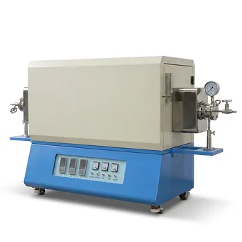
- Versatile Chemical Vapor Deposition Tube Furnace System for Advanced Material Research and Industrial Coating Processes
- Multi Heating Zones CVD Tube Furnace System for Precision Chemical Vapor Deposition and Advanced Material Synthesis
- HFCVD Machine System for Nano Diamond Coating on Drawing Dies and Industrial Tools
- Chemical Vapor Deposition CVD System Slide PECVD Tube Furnace with Liquid Gasifier PECVD Machine
- Split Chamber CVD Tube Furnace with Vacuum Station Chemical Vapor Deposition System Machine
People Also Ask
- How does a sliding rail design benefit the CVD process within a furnace ventilation hood? Enhance Control & Quenching
- What role do by-product desorption and evacuation play in CVD film quality? Key Factors for High-Purity Films
- How does the deposition process occur within a Chemical Vapor Deposition (CVD) reactor? Explore the 5-Stage Growth Cycle
- Why is CVD preferred over PVD for high-aspect-ratio features? Superior Conformality for Semiconductor Fabrication
- What is the primary function of a CVD system in the synthesis of Bi2O2Se thin films? Master High-Quality Crystal Growth

Tech Team · ThermUnits
Last updated on Apr 14, 2026
Related Products
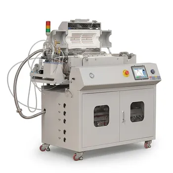
Versatile Chemical Vapor Deposition Tube Furnace System for Advanced Material Research and Industrial Coating Processes
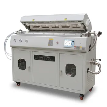
Multi Heating Zones CVD Tube Furnace System for Precision Chemical Vapor Deposition and Advanced Material Synthesis
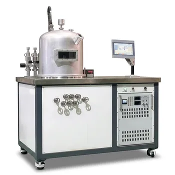
HFCVD Machine System for Nano Diamond Coating on Drawing Dies and Industrial Tools
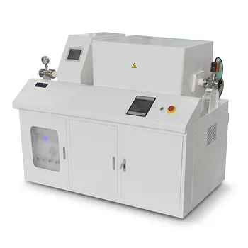
Chemical Vapor Deposition CVD System Slide PECVD Tube Furnace with Liquid Gasifier PECVD Machine
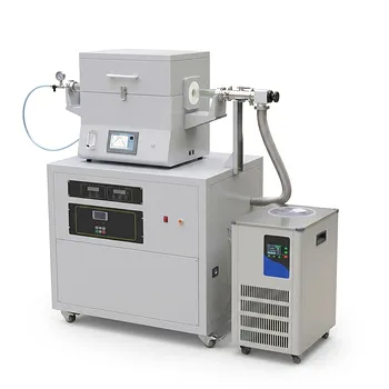
Split Chamber CVD Tube Furnace with Vacuum Station Chemical Vapor Deposition System Machine
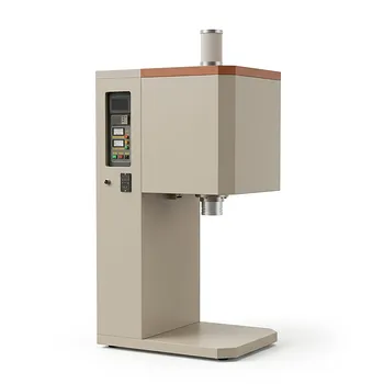
Vertical Openable Tube Furnace 0-1700c High Temperature Laboratory System for CVD and Vacuum Heat Treatment
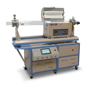
Dual Tube 100mm 80mm CVD Sliding Furnace with 4 Channel Gas Mixing and Vacuum System
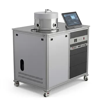
Inclined Rotary Plasma Enhanced Chemical Vapor Deposition PECVD System for Thin Film Deposition and Nanomaterial Synthesis
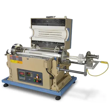
1200°C High Temperature 4 Inch Tube Furnace with Sliding Flange for CVD Systems
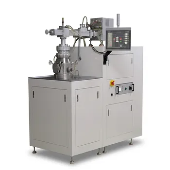
Cylindrical Resonator MPCVD Machine System for Microwave Plasma Chemical Vapor Deposition and Lab Diamond Growth
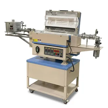
5 Inch Rotary Tube Furnace with Automatic Feeding and Receiving System 1200C Three Zone CVD Powder Processing
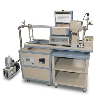
1200C Max Compact Auto-Sliding PECVD Furnace with 2 Inch Tube and Vacuum Pump
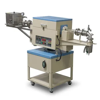
Two Zone Rotary CVD Furnace with Automatic Feeding and Receiving System for Powder Processing
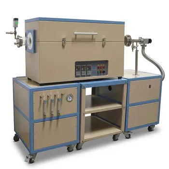
Three Zone Quartz Tube Furnace with 3 Channel Gas Mixer Vacuum Pump and Anti Corrosive Vacuum Gauge
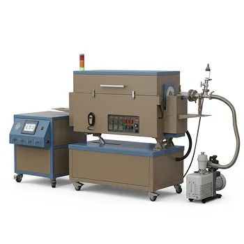
5 Inch Three Zone Rotary Tube Furnace with Integrated Gas Delivery System and 1200C Capability for Advanced Material CVD Processing
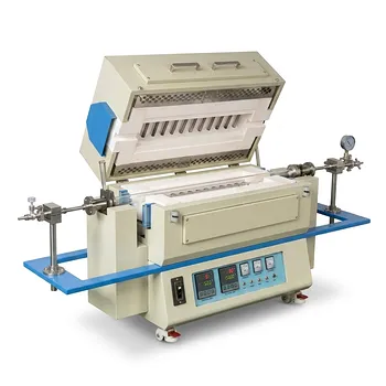
High Temperature Dual Zone Rotating Tube Furnace 1500C Silicon Carbide Heating for Advanced Material Synthesis
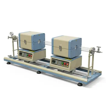
1200C Max Dual Sliding Tube Furnace with 50 mm Tube Flanges for CVD
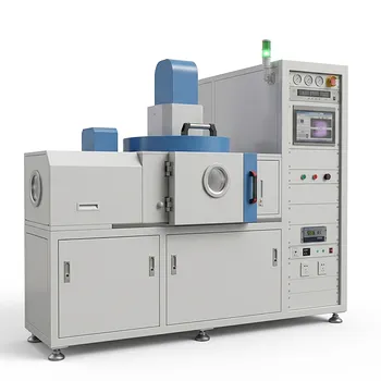
Radio Frequency Plasma Enhanced Chemical Vapor Deposition RF PECVD System for Laboratory and Industrial Thin Film Growth
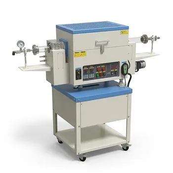
4 Inch Two Zone Rotary CVD Tube Furnace for High Temperature Battery Material Synthesis and Advanced Material Calcination