Why is vacuum annealing necessary for hexagonal Boron Nitride (hBN) samples? Achieve Atomically Clean Surfaces
Updated 3 months ago
Vacuum annealing is the critical purification step required to eliminate organic contaminants—specifically Polymethyl Methacrylate (PMMA) residues—that are inevitably left behind on hexagonal Boron Nitride (hBN) during the transfer process. By applying thermal treatment within a vacuum, researchers can achieve an atomically clean surface that is free of polymer artifacts.
This thermal process is essential because even microscopic residues can obscure atomic structures, making it impossible to perform high-resolution characterization. Vacuum annealing restores the intrinsic properties of the hBN, enabling sub-angstrom resolution imaging and the precise observation of point defects.
The Impact of Organic Contamination on hBN Characterization
Eliminating PMMA and Polymer Residues
During the transfer of hBN flakes, organic polymers like PMMA are used as support layers, but they leave a persistent film upon removal. Vacuum annealing provides the necessary thermal energy to break these polymer bonds and desorb them from the hBN surface without introducing new atmospheric impurities.
Enabling Sub-Angstrom Precision
For techniques like Scanning Transmission Electron Microscopy (STEM), any surface residue creates "noise" that interferes with the electron beam. A vacuum-annealed, atomically clean surface is the prerequisite for observing the actual point defect structures and atomic arrangements within the hBN lattice.
Achieving Atomic-Level Flatness
Beyond just removing chemicals, high-temperature treatment helps the hBN substrate reach a state of atomic-level flatness. This pristine physical environment is necessary if the hBN is to be used as a substrate for the subsequent growth of other nanostructures, such as carbon nanotubes or metal catalysts.
Enhancing Interface Quality and Device Performance
Reducing Contact Resistance
In the fabrication of Field-Effect Transistors (FETs), residues at the metal-semiconductor interface act as barriers to electron flow. Annealing at temperatures around 300°C in a vacuum promotes atomic rearrangement at these interfaces, significantly reducing contact resistance between the hBN and metal electrodes like gold or titanium.
Optimizing Carrier Mobility
By eliminating moisture and organic "traps" introduced during manufacturing, vacuum annealing improves the carrier mobility and the current on-off ratio of electronic devices. This ensures that the electrical testing reflects the true potential of the atomic-layer film rather than the limitations of a dirty interface.
Removing Native Oxide Layers
In cases where hBN is grown on substrates like germanium, vacuum or hydrogen annealing is used to strip away natural oxide layers. This restores a clean crystal surface, providing a high-quality template that facilitates the highly oriented growth of hBN nano-islands.
Understanding the Trade-offs and Limitations
Thermal Stress and Crystal Strain
While high temperatures are necessary for cleaning, they can introduce internal stresses or crystal defects if the cooling process is not carefully controlled. Rapid temperature changes may cause the hBN to shift or develop ripples due to differences in thermal expansion between the flake and its underlying substrate.
The Risk of Surface Degradation
Exceeding the stable temperature limit for a specific material system can lead to unintended consequences, such as the decomposition of the substrate or the unwanted diffusion of atoms into the hBN layer. Precise control over the vacuum level and temperature duration is required to balance cleanliness with structural integrity.
Strategic Implementation of Vacuum Annealing
How to Apply This to Your Project
To determine the optimal annealing parameters, you must align the thermal profile with your ultimate characterization or application goal.
- If your primary focus is Atomic-Resolution Imaging (STEM): Prioritize high-vacuum environments to ensure the complete removal of PMMA for a residue-free, sub-angstrom view of point defects.
- If your primary focus is High-Performance Electronics: Focus on a 300°C vacuum soak after electrode deposition to eliminate interface moisture and maximize carrier mobility.
- If your primary focus is Heteroepitaxial Growth: Utilize high-temperature hydrogen annealing to strip oxides from the growth template before the hBN deposition begins.
Through the calculated application of heat and vacuum, you transform a contaminated flake into a pristine platform for advanced nanoscience.
Summary Table:
| Application Goal | Primary Benefit | Recommended Process |
|---|---|---|
| Atomic Imaging (STEM) | Removes PMMA/polymer residues | High-vacuum thermal treatment |
| Electronic Devices | Reduces contact resistance & improves mobility | 300°C vacuum soak after transfer |
| Heteroepitaxial Growth | Strips native oxide layers from templates | High-temp hydrogen or vacuum anneal |
| Surface Science | Achieves atomic-level flatness | Controlled high-temperature profile |
Optimize Your hBN Research with THERMUNITS Precision Furnaces
Achieving an atomically clean surface requires precise thermal control and reliable vacuum environments. THERMUNITS is a leading manufacturer of high-temperature laboratory equipment specifically designed for material science and industrial R&D.
Whether you need to eliminate PMMA residues or strip native oxide layers, our comprehensive range of thermal solutions—including Vacuum, Atmosphere, Tube, and CVD/PECVD systems—provides the stability and performance your research demands. Our equipment is trusted by labs worldwide for dental, electronic, and nanostructure applications.
Ready to elevate your heat treatment precision?
Contact THERMUNITS Today to discuss your specific furnace requirements and see how our advanced thermal technology can accelerate your breakthroughs.
References
- Rohit Babar, Viktor Ivády. Low-symmetry vacancy-related spin qubit in hexagonal boron nitride. DOI: 10.1038/s41524-024-01361-z
Mentioned Products
- High Temperature 1000C Vacuum Furnace with 8 Inch ID Chamber for Material Sintering and Research Annealing
- High Temperature Cold Wall Vacuum Furnace for Advanced Material Sintering and Annealing 1600C Heating Area 200x200x300mm
- Double Temperature Zone Double Cover Tube Furnace for High Temperature CVD and Vacuum Annealing
- Three Temperature Zone High Temperature Vacuum Tube Furnace for CVD and Material Sintering
- High Temperature Vertical Atmosphere Controlled Furnace with Automatic Bottom Loading and 1700°C Capacity for Advanced Material Research
People Also Ask
- How does the temperature control precision of a high-temperature sintering furnace affect Na1+xLa1-xZr2O6-δ ceramics?
- How does a high-temperature sintering furnace environment enhance NdFeB magnets? Achieve 98%+ density with precision.
- What role does a high-temperature annealing furnace play in forming ordered Pt3(CoNi) intermetallic catalysts?
- What is the function of high-vacuum furnaces in (Mo2/3V1/3)n+1AlCn MAX phase synthesis? Ensure Purity & Diffusion.
- How does a vacuum or atmosphere sintering furnace contribute to the congener-welding process of carbon nitride membranes?

Tech Team · ThermUnits
Last updated on Jun 03, 2026
Related Products
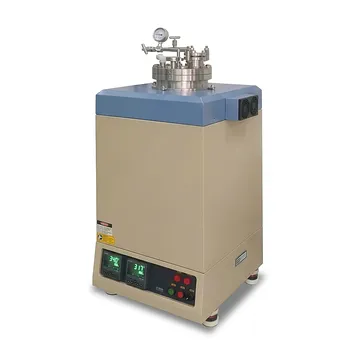
High Temperature 1000C Vacuum Furnace with 8 Inch ID Chamber for Material Sintering and Research Annealing
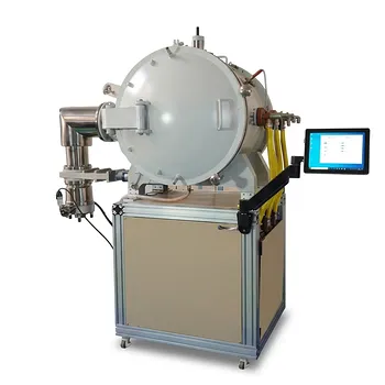
High Temperature Cold Wall Vacuum Furnace for Advanced Material Sintering and Annealing 1600C Heating Area 200x200x300mm
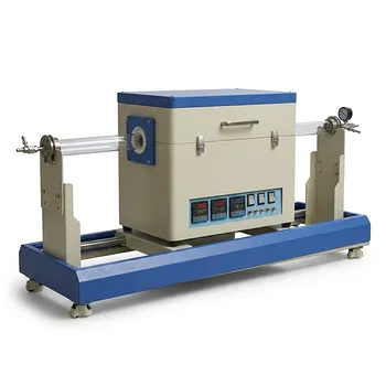
Double Temperature Zone Double Cover Tube Furnace for High Temperature CVD and Vacuum Annealing
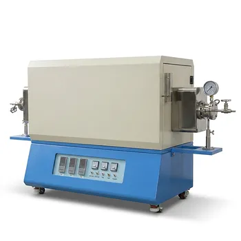
Three Temperature Zone High Temperature Vacuum Tube Furnace for CVD and Material Sintering
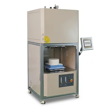
High Temperature Vertical Atmosphere Controlled Furnace with Automatic Bottom Loading and 1700°C Capacity for Advanced Material Research
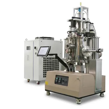
950C Rapid Thermal Processing Furnace for 12 Inch Wafer CSS Coating with Rotating Substrate Holder
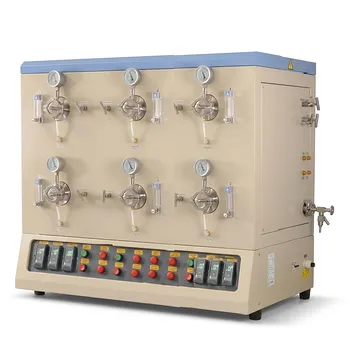
1200C High Throughput Multi Channel Tube Furnace with 50mm Quartz Tubes for Annealing and Material Phase Diagram Research
Compact Atmosphere Controlled Rapid Thermal Processing RTP Furnace with 4 Inch ID Quartz Tube 1100C
High Temperature Vacuum Lamination Hot Press Furnace Machine for Semiconductor Wafer Bonding and Advanced Composite Thermal Processing
2500C High Vacuum Ultrafast Heating Pellet Press with Automated 8 Sample Loading System
Bottom Loading Vacuum Furnace 1200C Rapid Cooling Atmosphere Control Quartz Chamber
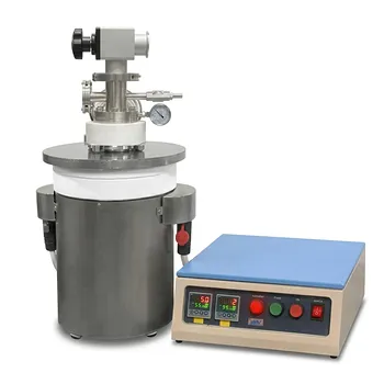
1100C High Temperature Vacuum Crucible Furnace with Quartz Chamber for Thermal Processing and Sintering
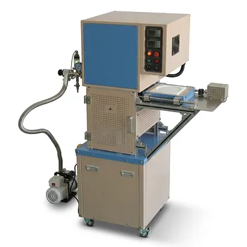
1200°C Bottom Loading Vacuum Furnace with Rapid Gas Cooling and 8.6 Inch Diameter Quartz Chamber
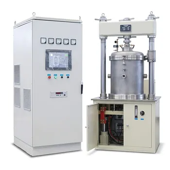
Industrial Vacuum Hot Press Furnace Machine and High Temperature Heated Vacuum Press for Advanced Material Sintering
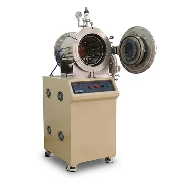
High Temperature Cold Wall High Vacuum Chamber Furnace 1400C for Advanced Material Processing
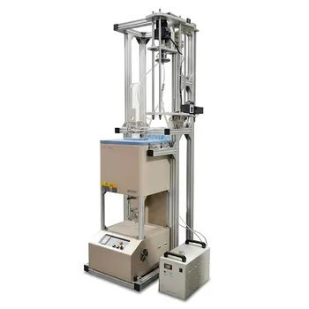
500C Vacuum Vertical Tube Furnace 84mm OD Sample Rotation Lifting System
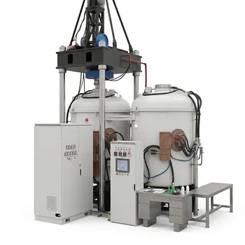
High Pressure 600T Vacuum Induction Hot Press Furnace for Advanced Material Heat Treatment and Sintering
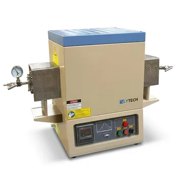
1800C High Temperature Compact Vacuum Tube Furnace with 60mm OD Alumina Tube and Kanthal MoSi2 Heating Elements
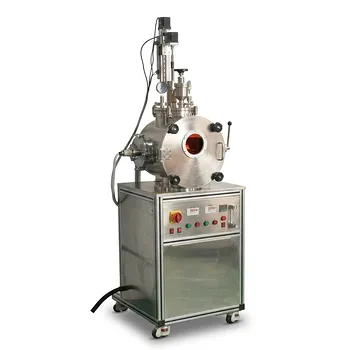
High Vacuum Melting Casting Furnace with Mechanical Stirring and Secondary Charge for Metallic Alloy Research