How does Chemical Vapor Deposition (CVD) ensure high quality in optical thin film? Master Precision & Atomic Control
Updated 3 months ago
Chemical Vapor Deposition (CVD) is the gold standard for high-performance optics. It achieves superior quality by enabling atomic-level control over film thickness, chemical composition, and refractive index. This precision results in films with ultra-low absorption rates (less than 0.1%) and high uniformity across complex or large-scale substrates.
Core Takeaway: CVD ensures optical and optoelectronic quality by utilizing precise gas-phase reactions to grow high-purity, conformal thin films. This level of control allows engineers to tailor material properties—such as crystal orientation and stoichiometry—to meet exact wavelength and detectivity requirements.
Precision Control of Optical Properties
Achieving Atomic-Level Thickness and Uniformity
CVD systems utilize high-precision mass flow controllers to regulate the entry ratio of reaction precursors. This ensures that the chemical reactions occur at a consistent rate across the substrate, resulting in films with uniform thickness even over large areas like architectural glass.
Engineering the Refractive Index
For multilayer optical stacks, the ability to manipulate the refractive index is critical. By adjusting gas flow ratios and furnace pressure, CVD allows for the precise tuning of the film's chemical stoichiometry, ensuring the material interacts with light exactly as designed.
Minimizing Optical Absorption
High-quality optical films require low absorption rates to prevent energy loss and signal degradation. CVD processes can consistently achieve absorption levels below 0.1%, which is essential for high-power laser optics and sensitive infrared detectors.
Advancements in Optoelectronic Performance
High-Purity Epitaxial Growth
In optoelectronics, techniques like Metal-Organic CVD (MOCVD) are used to grow high-purity epitaxial layers. Materials such as mercury cadmium telluride (HgCdTe) can be grown with tailored compositions for specific wavelengths, ensuring minimal defect density and high detectivity.
Superior Conformality and Step Coverage
Unlike physical deposition methods, CVD offers excellent step coverage, allowing for the uniform coating of complex three-dimensional microstructures. This is vital for integrating optical functions into modern semiconductor architectures and photonic crystal fibers.
Molecular and Crystalline Order
The stable thermal fields provided by multi-zone temperature control facilitate ordered crystal growth. This results in highly crystalline monolayer or few-layer structures, which are necessary for the synthesis of functional materials like graphene and carbon nanotubes.
Understanding the Trade-offs
The Thermal Budget Challenge
Standard thermal CVD often requires high temperatures to trigger chemical reactions, which can limit the types of substrates used. While high heat ensures strong adhesion and crystallinity, it may damage heat-sensitive components or cause unwanted diffusion between layers.
Precursor Toxicity and Complexity
The precursors used in CVD are often volatile, corrosive, or toxic gases. This necessitates complex delivery systems and rigorous safety protocols, which can increase the operational cost and infrastructure requirements compared to simpler deposition methods.
Plasma-Enhanced Alternatives
To mitigate high temperatures, Plasma-Enhanced CVD (PECVD) is used to lower the activation energy of reactions. However, while PECVD protects sensitive substrates, it may sometimes introduce higher levels of impurities or structural defects compared to high-temperature thermal CVD.
How to Apply This to Your Project
Making the Right Choice for Your Goal
To maximize the benefits of CVD in your application, consider the specific requirements of your optical or electronic system.
- If your primary focus is high-power laser optics: Prioritize high-temperature thermal CVD to ensure the lowest possible absorption rates and maximum film density.
- If your primary focus is heat-sensitive semiconductor integration: Utilize PECVD to achieve high-quality ultrathin films without exceeding the thermal limits of your substrate.
- If your primary focus is infrared sensing or LEDs: Use MOCVD to grow epitaxial layers with tailored bandgaps and minimal crystalline defects.
- If your primary focus is complex 3D microstructures: Leverage the superior conformality of gas-phase CVD to ensure uniform coating on internal channels and vertical sidewalls.
By mastering the variables of gas flow, pressure, and temperature, CVD transforms chemical precursors into the high-performance building blocks of modern photonics.
Summary Table:
| CVD Method | Key Advantage | Ideal Application |
|---|---|---|
| Thermal CVD | Maximum density & lowest absorption | High-power laser optics |
| PECVD | Low activation energy/temperature | Heat-sensitive substrates |
| MOCVD | High-purity epitaxial growth | LEDs & Infrared detectors |
| Gas-Phase CVD | Exceptional step coverage | 3D microstructures & fibers |
As a leading manufacturer of high-temperature laboratory equipment, THERMUNITS empowers material science and industrial R&D with the precision needed for superior thin-film deposition. Our comprehensive range of solutions—including CVD/PECVD systems, Muffle, Vacuum, and Tube furnaces—is engineered to provide the stable thermal fields and gas-phase control essential for high-quality optical applications. Contact our experts today to find the perfect thermal processing solution to enhance your research and production efficiency.
Mentioned Products
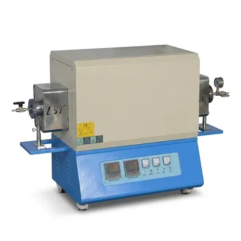
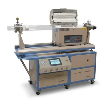
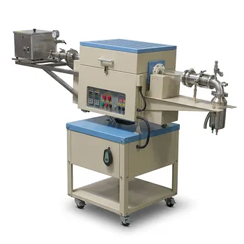
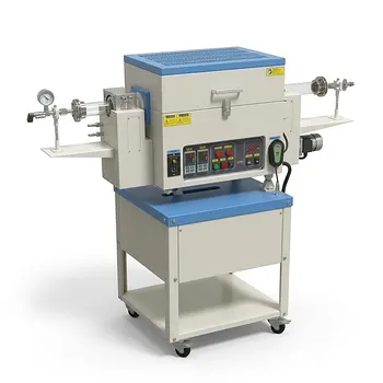
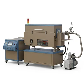
- Multi Heating Zones CVD Tube Furnace System for Precision Chemical Vapor Deposition and Advanced Material Synthesis
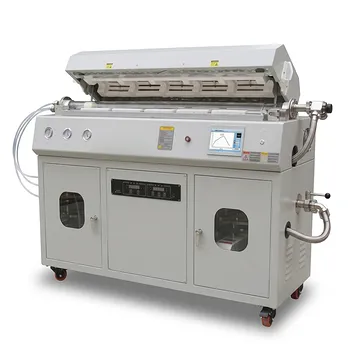
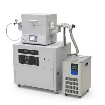
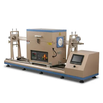
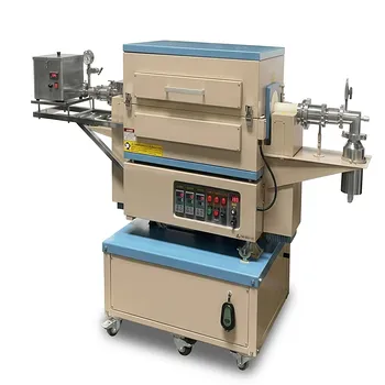
- Chemical Vapor Deposition CVD System Slide PECVD Tube Furnace with Liquid Gasifier PECVD Machine
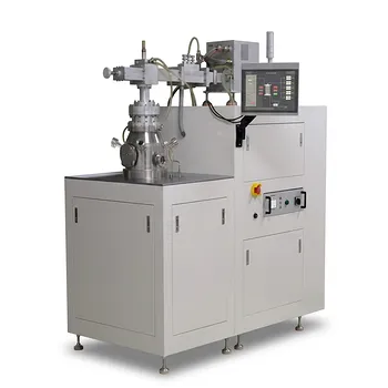
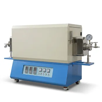
- High Temperature 1700C Tube Furnace with High Vacuum Turbomolecular Pump System and Multi Channel Mass Flow Controller Gas Mixer
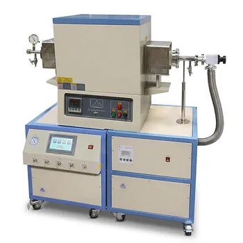
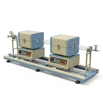
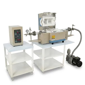
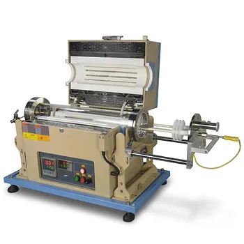
- Dual Tube 100mm 80mm CVD Sliding Furnace with 4 Channel Gas Mixing and Vacuum System
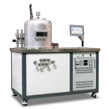
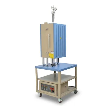
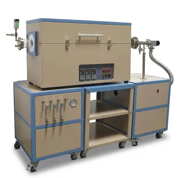
- Split Chamber CVD Tube Furnace with Vacuum Station Chemical Vapor Deposition System Machine
People Also Ask
- How does the use of helium gas flow control affect the DM process? Enhance Precision in CVD Graphene Synthesis
- How does the deposition process occur within a Chemical Vapor Deposition (CVD) reactor? Explore the 5-Stage Growth Cycle
- What are the primary differences between hot-wall and cold-wall CVD reactors? Choose the Best System for High Purity
- How does the Sweet Spot region within a chemical vapor deposition reactor influence the morphology control of VOx particles?
- What is the primary role of a High-Vacuum CVD tube furnace? Enabling Precise Semiconductor Micro-tripod Growth.
Tech Team · ThermUnits
Last updated on Apr 14, 2026
Related Products
Multi Heating Zones CVD Tube Furnace System for Precision Chemical Vapor Deposition and Advanced Material Synthesis
Chemical Vapor Deposition CVD System Slide PECVD Tube Furnace with Liquid Gasifier PECVD Machine
High Temperature 1700C Tube Furnace with High Vacuum Turbomolecular Pump System and Multi Channel Mass Flow Controller Gas Mixer
Dual Tube 100mm 80mm CVD Sliding Furnace with 4 Channel Gas Mixing and Vacuum System
Split Chamber CVD Tube Furnace with Vacuum Station Chemical Vapor Deposition System Machine
Vertical Openable Tube Furnace 0-1700c High Temperature Laboratory System for CVD and Vacuum Heat Treatment
1200C Max Dual Sliding Tube Furnace with 50 mm Tube Flanges for CVD
Two Zone Rotary CVD Furnace with Automatic Feeding and Receiving System for Powder Processing
Cylindrical Resonator MPCVD Machine System for Microwave Plasma Chemical Vapor Deposition and Lab Diamond Growth
Two Zone Rotary Tube Furnace for Powder CVD Coating and Core Shell Material Synthesis 1100C
HFCVD Machine System for Nano Diamond Coating on Drawing Dies and Industrial Tools
4 Inch Two Zone Rotary CVD Tube Furnace for High Temperature Battery Material Synthesis and Advanced Material Calcination
1200C Sliding Tube Furnace for Rapid Thermal Processing and CVD Graphene Growth with 100mm OD Capacity
Three Temperature Zone High Temperature Vacuum Tube Furnace for CVD and Material Sintering
1200C Three Zone Vertical Tube Furnace with 2 Inch Quartz Tube and Vacuum Flanges
5 Inch Three Zone Rotary Tube Furnace with Integrated Gas Delivery System and 1200C Capability for Advanced Material CVD Processing
1200°C High Temperature 4 Inch Tube Furnace with Sliding Flange for CVD Systems
Three Zone Quartz Tube Furnace with 3 Channel Gas Mixer Vacuum Pump and Anti Corrosive Vacuum Gauge
1500C 3-Zone Rotary Tube Furnace 60mm with Automatic Powder Feeding and Receiving System for Continuous Material Synthesis