What technical advantages do CVD machines provide for the synthesis of nanomaterials? Precision Growth & Superior Quality
Updated 3 months ago
Chemical Vapor Deposition (CVD) machines offer unparalleled control over the atomic-level synthesis of nanomaterials by integrating precise thermal, atmospheric, and chemical parameters. This capability enables the production of high-quality, large-area graphene and aligned carbon nanotubes with specific electronic and structural properties. By manipulating precursor flow, temperature, and reaction time, CVD systems provide a scalable pathway to materials that exhibit superior carrier mobility and structural uniformity.
CVD machines transform complex chemical reactions into a repeatable manufacturing process, allowing for the precise tuning of nanomaterial morphology and electrical performance through the rigorous control of growth environments.
Precision Regulation of Growth Parameters
Atmospheric Control via Mass Flow Controllers
High-precision CVD systems utilize multi-channel mass flow controllers (MFCs) to accurately regulate the ratios of precursor gases like methane, ethylene, and hydrogen. This allows for the exact management of carbon source decomposition and the reduction of impurities during the deposition process.
Precise gas flow regulation ensures the construction of interconnected three-dimensional conductive networks. This is essential for applications such as silicon-based anodes, where electrical conductivity depends on the structural integrity of the carbon network.
Thermal Field Stability and Sudden Initiation
CVD machines maintain stable thermal fields, often reaching temperatures around 850 °C to 1000 °C, to facilitate catalytic decomposition. Advanced systems feature mechanisms for sudden initiation, moving samples rapidly into the high-temperature zone to subject catalysts to an instantaneous thermal shock.
This thermal shock effectively suppresses catalyst agglomeration, preserving the small particle size and high activity of the catalyst. As a result, engineers can achieve higher carbon yields and more precise regulation of carbon nanotube diameters.
Achieving Superior Material Quality and Scale
Large-Area Single-Crystal Synthesis
One of the most significant technical advantages of CVD is the ability to produce large-area, high-quality nanomaterials. For example, the process can synthesize single-crystal graphene sheets with dimensions exceeding 15 cm.
These large-area materials maintain exceptional electronic properties, such as carrier mobility exceeding 200,000 cm²/V·s. This makes CVD the preferred method for producing materials intended for high-performance advanced electronics and optoelectronics.
Atomic-Level Thickness and Uniformity
CVD and PECVD (Plasma-Enhanced CVD) systems enable atomic-level thickness control across the entire substrate. This precision can reduce film thickness fluctuations to within 5 percent, ensuring consistency in mass production.
The ability to produce high-purity, dense, and uniform films is critical for the development of precision sensors and semiconductor devices. These systems allow for high performance even when processing at lower temperatures through the use of plasma energy.
Structural and Functional Customization
Direct Growth and Alignment
CVD allows for the growth of aligned carbon nanotubes (CNTs) and nanowires directly onto catalytic substrates. This directional growth is managed by adjusting process variables such as pressure, gas ratios, and the specific orientation of the catalyst.
The system's control over the alignment, density, and length of nanostructures facilitates the creation of customized surfaces. This is vital for applications requiring specific mechanical or thermal interface properties.
In-Situ Doping and Bandgap Engineering
Modern CVD hardware facilitates in-situ doping and alloying during the growth phase. By introducing specific precursors during the reaction, engineers can customize the bandgaps and surface functionalities of the nanomaterials.
This capability is essential for creating materials used in energy storage and advanced sensors. It eliminates the need for post-processing steps that could potentially damage the delicate nanostructures.
Understanding the Trade-offs
Catalyst Dependency and Contamination
The quality of CVD-grown nanomaterials is heavily dependent on the purity and morphology of the metal catalyst. Residues from these catalysts can sometimes remain in the final product, which may interfere with sensitive electronic or biomedical applications.
Energy Consumption and Precursor Hazards
Maintaining high-vacuum environments and sustained high temperatures requires significant energy input, which can impact the cost-effectiveness of the process. Additionally, the precursors used—such as methane, ethylene, and hydrogen—are often flammable or toxic, requiring sophisticated safety and exhaust handling systems.
How to Apply This to Your Project
When selecting a CVD approach for nanomaterial synthesis, your choice should be driven by your specific performance and scale requirements.
- If your primary focus is high-performance electronics: Prioritize a system with high thermal stability and precise MFCs to achieve the carrier mobility and single-crystal quality required for semiconductor applications.
- If your primary focus is large-scale production of CNTs: Look for systems capable of "sudden initiation" to prevent catalyst agglomeration and ensure uniform tube diameters across large batches.
- If your primary focus is temperature-sensitive substrates: Utilize PECVD (Plasma-Enhanced CVD) to achieve high-quality film growth at lower processing temperatures than standard thermal CVD.
By mastering the tunable parameters of CVD technology, you can transition from basic material synthesis to the engineering of high-performance, functional nanostructures tailored to specific industrial needs.
Summary Table:
| Technical Advantage | Description | Industrial Impact |
|---|---|---|
| Atmospheric Control | Multi-channel MFCs regulate precise precursor gas ratios | High-purity, interconnected 3D conductive networks |
| Thermal Stability | 850°C–1000°C range with "sudden initiation" mechanisms | Prevents catalyst agglomeration; ensures uniform CNT diameters |
| Atomic-level Precision | Thickness fluctuations controlled within 5% | Consistent performance for sensors and semiconductors |
| In-situ Customization | Integrated doping and directional alignment growth | Tailored bandgaps for advanced energy storage and electronics |
Accelerate Your Nanotechnology Research with THERMUNITS
As a global leader in high-temperature laboratory equipment, THERMUNITS provides the precision tools required for cutting-edge material science. Our advanced CVD and PECVD systems are specifically engineered to offer the thermal stability and atmospheric control necessary for synthesizing high-quality graphene, carbon nanotubes, and other nanomaterials.
Why Choose THERMUNITS for Your R&D?
- Comprehensive Range: We offer everything from Muffle, Vacuum, and Tube furnaces to specialized Rotary, Hot Press, and Vacuum Induction Melting (VIM) systems.
- Unmatched Precision: Our equipment is designed for rigorous industrial R&D, ensuring repeatable results and atomic-level uniformity.
- Scalable Solutions: Whether you need a benchtop Dental Furnace or a large-scale Electric Rotary Kiln, we provide thermal processing excellence.
Ready to enhance your lab's synthesis capabilities? Contact our experts today to discuss your specific heat treatment requirements!
Mentioned Products
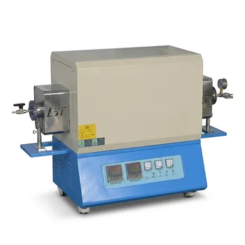
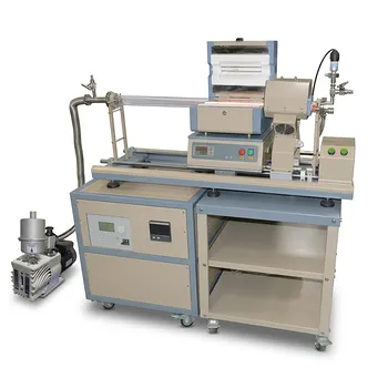
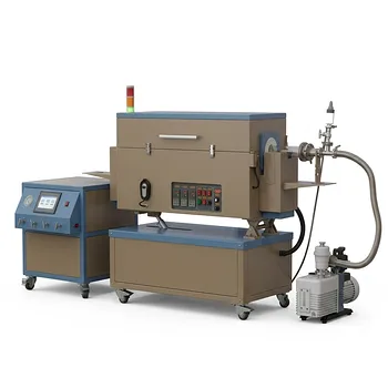
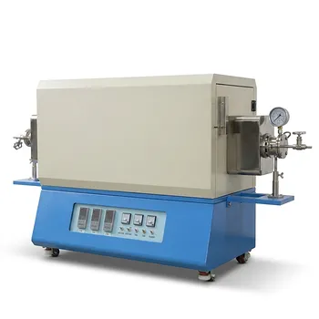
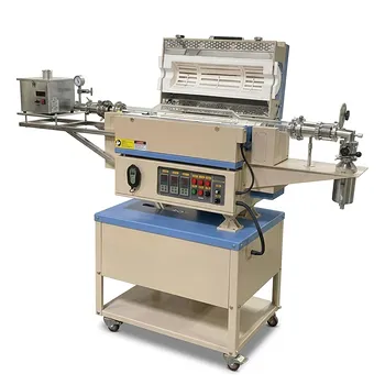
- HFCVD Machine System for Nano Diamond Coating on Drawing Dies and Industrial Tools
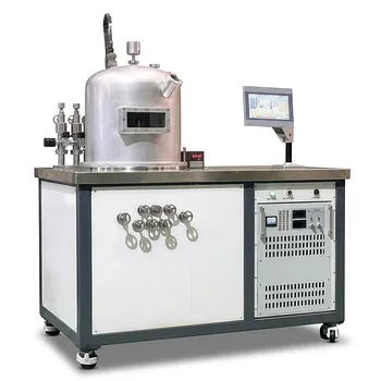
- Cylindrical Resonator MPCVD Machine System for Microwave Plasma Chemical Vapor Deposition and Lab Diamond Growth
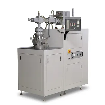
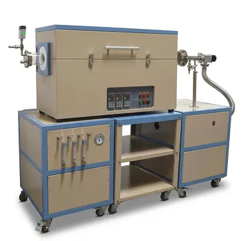
- Split Chamber CVD Tube Furnace with Vacuum Station Chemical Vapor Deposition System Machine
- 915MHz MPCVD Diamond Machine Microwave Plasma Chemical Vapor Deposition System Reactor
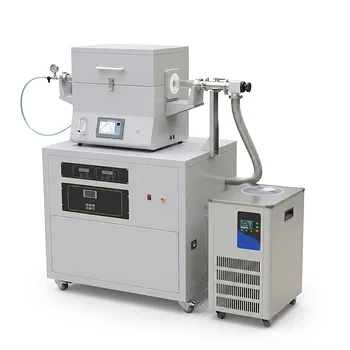
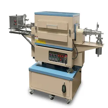
- Two Zone Rotary CVD Furnace with Automatic Feeding and Receiving System for Powder Processing
People Also Ask
- How does the use of helium gas flow control affect the DM process? Enhance Precision in CVD Graphene Synthesis
- What technical advantages does a CVD system offer for intermetallics? Achieve Atomic-Level Precision & Phase Purity
- What role do by-product desorption and evacuation play in CVD film quality? Key Factors for High-Purity Films
- How does a Chemical Vapor Deposition (CVD) system ensure product quality? Precision Control for 2D Nanomaterial Growth
- What is the fundamental working principle of a Chemical Vapor Deposition (CVD) machine? Master Precision Film Growth
Tech Team · ThermUnits
Last updated on Apr 14, 2026
Related Products
HFCVD Machine System for Nano Diamond Coating on Drawing Dies and Industrial Tools
Cylindrical Resonator MPCVD Machine System for Microwave Plasma Chemical Vapor Deposition and Lab Diamond Growth
Split Chamber CVD Tube Furnace with Vacuum Station Chemical Vapor Deposition System Machine
915MHz MPCVD Diamond Machine Microwave Plasma Chemical Vapor Deposition System Reactor
Two Zone Rotary CVD Furnace with Automatic Feeding and Receiving System for Powder Processing
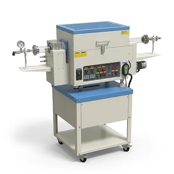
Multi Heating Zones CVD Tube Furnace System for Precision Chemical Vapor Deposition and Advanced Material Synthesis
Vertical Openable Tube Furnace 0-1700c High Temperature Laboratory System for CVD and Vacuum Heat Treatment
High Temperature 1700C Tube Furnace with High Vacuum Turbomolecular Pump System and Multi Channel Mass Flow Controller Gas Mixer
1200C Max Dual Sliding Tube Furnace with 50 mm Tube Flanges for CVD
Dual Tube 100mm 80mm CVD Sliding Furnace with 4 Channel Gas Mixing and Vacuum System
1200°C High Temperature 4 Inch Tube Furnace with Sliding Flange for CVD Systems
1200C Max Compact Auto-Sliding PECVD Furnace with 2 Inch Tube and Vacuum Pump
5 Inch Three Zone Rotary Tube Furnace with Integrated Gas Delivery System and 1200C Capability for Advanced Material CVD Processing
Three Temperature Zone High Temperature Vacuum Tube Furnace for CVD and Material Sintering
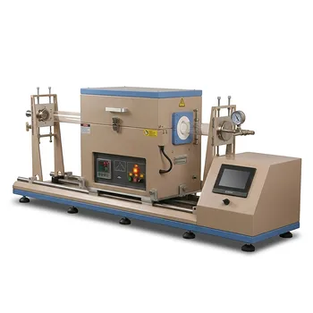
5 Inch Rotary Tube Furnace with Automatic Feeding and Receiving System 1200C Three Zone CVD Powder Processing
Three Zone Quartz Tube Furnace with 3 Channel Gas Mixer Vacuum Pump and Anti Corrosive Vacuum Gauge
4 Inch Two Zone Rotary CVD Tube Furnace for High Temperature Battery Material Synthesis and Advanced Material Calcination
1500C 3-Zone Rotary Tube Furnace 60mm with Automatic Powder Feeding and Receiving System for Continuous Material Synthesis
1200C Sliding Tube Furnace for Rapid Thermal Processing and CVD Graphene Growth with 100mm OD Capacity