In what ways does Chemical Vapor Deposition (CVD) improve solar cells? Enhance Efficiency with Precise Thin-Film Coating
Updated 3 months ago
Chemical Vapor Deposition (CVD) is a cornerstone of modern photovoltaic manufacturing. It enhances efficiency by depositing precise, high-purity layers that capture more light and prevent electrical energy losses, while simultaneously boosting stability through robust protective coatings. By utilizing controlled gas-phase reactions, CVD creates the uniform films necessary for high-performance silicon and thin-film solar technologies to operate reliably for decades.
Core Takeaway: CVD improves solar cell performance by enabling superior surface passivation and light-trapping architectures. This process reduces electron losses and maximizes photon absorption, making it essential for high-efficiency cell designs like PERC, TOPCon, and Heterojunction (HJT).
Optimizing Light Management through Precision Coatings
The Role of Anti-Reflective Coatings (ARC)
CVD, particularly Plasma-Enhanced CVD (PECVD), is used to apply silicon nitride (SiNx) coatings to the surface of silicon wafers. These layers function as anti-reflective coatings that significantly reduce the amount of sunlight bouncing off the cell. By capturing more photons, the cell can convert a higher percentage of available solar energy into electricity.
Enhancing Transparency with Carbon Nanotubes
CVD is the preferred method for synthesizing high-purity carbon nanotubes (CNTs) used in transparent conductive electrodes. Unlike other methods that produce impurities, CVD-grown nanotubes offer 98% purity and excellent structural consistency. This results in higher optical transparency and better carrier mobility, allowing light to pass through while efficiently moving electrical charges.
Precise Control Over Film Thickness
The CVD process allows for atomic-level control over the thickness and composition of deposited films. This precision ensures that coatings are uniform even on textured or large-area substrates. Uniformity is critical for maintaining consistent performance across the entire surface of a solar module.
Maximizing Electrical Performance via Passivation
Reducing Electron Recombination Losses
Surface passivation is perhaps the most critical contribution of CVD to solar efficiency. CVD-deposited layers, such as hydrogen-rich SiNx, chemically "deactivate" defects on the silicon surface. This reduces surface recombination velocity, preventing electrons from being lost before they can be collected as current.
Extending Minority Carrier Lifetime
By providing superior surface passivation, CVD processes significantly improve the minority carrier lifetime within the silicon. When carriers last longer, the probability of them reaching the electrical contacts increases. This directly translates to higher open-circuit voltages and overall conversion efficiency.
Enabling Advanced Cell Architectures
Modern high-efficiency cells, including PERC, TOPCon, and HJT, rely on CVD for complex passivation stacks. These architectures use CVD to deposit intrinsic and doped amorphous silicon layers or transparent conductive oxides (TCOs). These layers are essential for creating the selective contacts that define next-generation photovoltaics.
Material Purity and Structural Consistency
Superiority Over Physical Vapor Deposition (PVD)
Unlike PVD, which relies on physical evaporation, CVD uses thermal decomposition or chemical reduction of precursor gases. This chemical approach results in higher-purity solid films with fewer structural defects. Higher purity is essential for maintaining the integrity of the semiconductor layers over the long term.
High-Throughput Manufacturing Stability
CVD equipment is designed for high-throughput production, which is vital for the scalability of solar technology. The process supports the creation of monocrystalline or epitaxial films that are highly stable under environmental stress. This stability ensures that the solar module maintains its efficiency rating throughout its 25-to-30-year lifespan.
Understanding the Trade-offs
Process Complexity and Cost
While CVD offers superior film quality, it often requires sophisticated vacuum systems and precise gas handling. The initial capital expenditure for PECVD or atmospheric CVD equipment can be higher than simpler coating methods. Furthermore, the cost of high-purity precursor gases adds to the operational overhead.
Thermal Budget and Substrate Sensitivity
Standard CVD processes often require high temperatures to facilitate chemical reactions, which can limit the types of substrates used. While PECVD solves this by using plasma to drive reactions at lower temperatures, the plasma itself can sometimes cause "ion bombardment" damage to sensitive substrates. Engineers must carefully balance temperature and plasma power to avoid degrading the very layers they are trying to protect.
Handling Volatile Precursors
The chemical precursors used in CVD are often volatile, flammable, or toxic. Managing these gases requires rigorous safety protocols and specialized abatement systems to treat exhaust gases. This adds a layer of regulatory and safety complexity to the manufacturing facility compared to physical deposition methods.
Making the Right Choice for Your Goal
How to Apply This to Your Project
CVD is not a one-size-fits-all solution, but it is indispensable for specific performance benchmarks.
- If your primary focus is Maximum Efficiency (PERC/TOPCon): Utilize PECVD for silicon nitride passivation and anti-reflective coatings to minimize recombination.
- If your primary focus is Next-Gen Tandem Cells: Invest in CVD for high-purity TCO underlayers and carbon nanotubes to ensure maximum transparency and conductivity.
- If your primary focus is Cost-Effective Mass Production: Evaluate high-throughput atmospheric CVD systems that can handle large-area substrates without the need for high-vacuum environments.
By leveraging the precision and purity of CVD, manufacturers can push the theoretical limits of solar energy conversion while ensuring long-term field reliability.
Summary Table:
| Feature | Solar Cell Benefit | Key Application |
|---|---|---|
| Anti-Reflective Coating | Maximizes photon capture and absorption | Silicon Nitride (SiNx) layers |
| Surface Passivation | Reduces electron loss and recombination | PERC, TOPCon, HJT architectures |
| Atomic-Level Control | Ensures uniform thickness on large substrates | Transparent conductive oxides |
| High-Purity Films | Enhances long-term structural stability | Carbon Nanotubes, epitaxial films |
Elevate Your Material Science R&D with THERMUNITS
As a leading manufacturer of high-temperature laboratory equipment, THERMUNITS provides the precision tools needed for advanced photovoltaic research. Our comprehensive range of thermal processing solutions—including CVD/PECVD systems, Tube, Vacuum, and Muffle furnaces—is designed to help industrial R&D teams achieve superior surface passivation and high-purity film deposition.
Ready to optimize your solar cell efficiency and stability? Contact our experts today at THERMUNITS to find the perfect heat treatment solution for your laboratory!
Mentioned Products
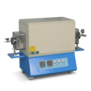
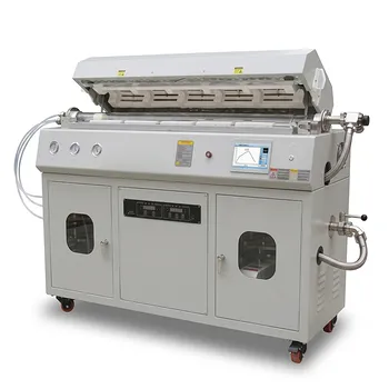
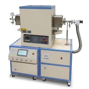
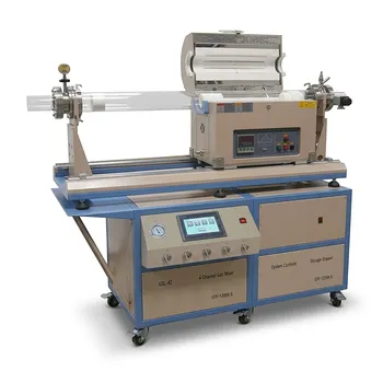
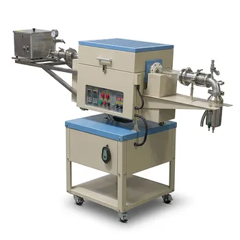
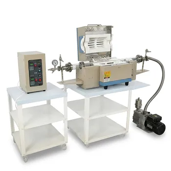
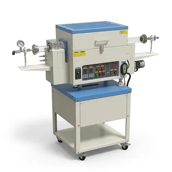
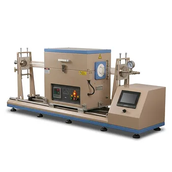
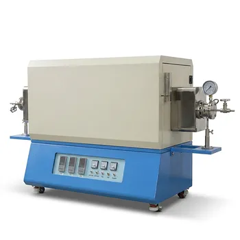
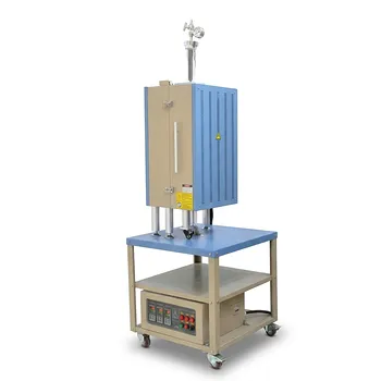
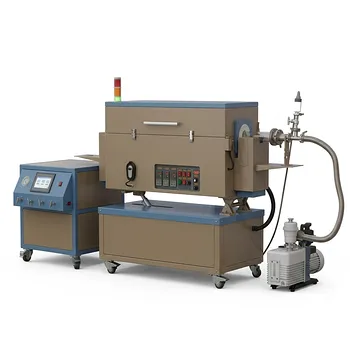
- Multi Heating Zones CVD Tube Furnace System for Precision Chemical Vapor Deposition and Advanced Material Synthesis
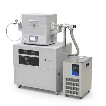
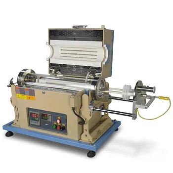
- Chemical Vapor Deposition CVD System Slide PECVD Tube Furnace with Liquid Gasifier PECVD Machine
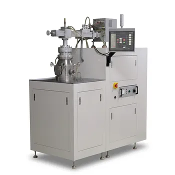
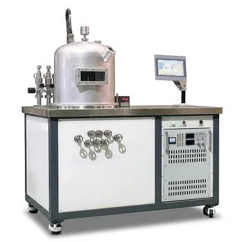
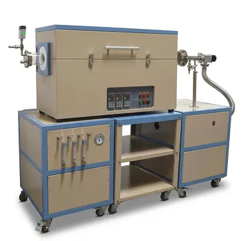
- High Temperature 1700C Tube Furnace with High Vacuum Turbomolecular Pump System and Multi Channel Mass Flow Controller Gas Mixer
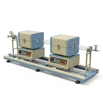
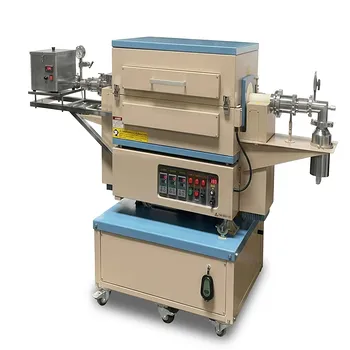
- Dual Tube 100mm 80mm CVD Sliding Furnace with 4 Channel Gas Mixing and Vacuum System
- Split Chamber CVD Tube Furnace with Vacuum Station Chemical Vapor Deposition System Machine
People Also Ask
- How does a Chemical Vapor Deposition (CVD) system ensure product quality? Precision Control for 2D Nanomaterial Growth
- How does the deposition process occur within a Chemical Vapor Deposition (CVD) reactor? Explore the 5-Stage Growth Cycle
- What role do by-product desorption and evacuation play in CVD film quality? Key Factors for High-Purity Films
- What technical advantages does a CVD system offer for intermetallics? Achieve Atomic-Level Precision & Phase Purity
- What is the primary role of a High-Vacuum CVD tube furnace? Enabling Precise Semiconductor Micro-tripod Growth.
Tech Team · ThermUnits
Last updated on Apr 14, 2026
Related Products
Multi Heating Zones CVD Tube Furnace System for Precision Chemical Vapor Deposition and Advanced Material Synthesis
Chemical Vapor Deposition CVD System Slide PECVD Tube Furnace with Liquid Gasifier PECVD Machine
High Temperature 1700C Tube Furnace with High Vacuum Turbomolecular Pump System and Multi Channel Mass Flow Controller Gas Mixer
Dual Tube 100mm 80mm CVD Sliding Furnace with 4 Channel Gas Mixing and Vacuum System
Split Chamber CVD Tube Furnace with Vacuum Station Chemical Vapor Deposition System Machine
Vertical Openable Tube Furnace 0-1700c High Temperature Laboratory System for CVD and Vacuum Heat Treatment
1200C Max Dual Sliding Tube Furnace with 50 mm Tube Flanges for CVD
Two Zone Rotary CVD Furnace with Automatic Feeding and Receiving System for Powder Processing
Cylindrical Resonator MPCVD Machine System for Microwave Plasma Chemical Vapor Deposition and Lab Diamond Growth
Two Zone Rotary Tube Furnace for Powder CVD Coating and Core Shell Material Synthesis 1100C
HFCVD Machine System for Nano Diamond Coating on Drawing Dies and Industrial Tools
4 Inch Two Zone Rotary CVD Tube Furnace for High Temperature Battery Material Synthesis and Advanced Material Calcination
1200C Sliding Tube Furnace for Rapid Thermal Processing and CVD Graphene Growth with 100mm OD Capacity
Three Temperature Zone High Temperature Vacuum Tube Furnace for CVD and Material Sintering
1200C Three Zone Vertical Tube Furnace with 2 Inch Quartz Tube and Vacuum Flanges
5 Inch Three Zone Rotary Tube Furnace with Integrated Gas Delivery System and 1200C Capability for Advanced Material CVD Processing
1200°C High Temperature 4 Inch Tube Furnace with Sliding Flange for CVD Systems
Three Zone Quartz Tube Furnace with 3 Channel Gas Mixer Vacuum Pump and Anti Corrosive Vacuum Gauge
1500C 3-Zone Rotary Tube Furnace 60mm with Automatic Powder Feeding and Receiving System for Continuous Material Synthesis