What are the advantages of using a cold-wall Rapid Thermal Processing (RTP) furnace? Superior Quality & Efficiency
Updated 1 month ago
Cold-wall Rapid Thermal Processing (RTP) furnaces revolutionize selenization by combining high-intensity infrared heating with reactive gas chemistry. This approach allows for processing at lower temperatures (approximately 650°C) and significantly shorter durations (1-2 hours) compared to traditional solid-source methods. By minimizing the thermal budget, RTP ensures superior wafer-scale uniformity and preserves the structural integrity of sensitive substrates.
The core advantage of cold-wall RTP in $H_2Se$ selenization is the ability to achieve high-quality, photovoltaic-grade material growth through precise, millisecond-level thermal control. This system maximizes production efficiency while preventing the uncontrolled elemental diffusion and material degradation typical of slower, high-heat processes.
Optimizing the Thermal Budget and Efficiency
Dramatic Reduction in Processing Time
Unlike solid-source processes that rely on slow ramp rates, RTP uses infrared lamp arrays for ultra-fast heating and cooling. This technology enables the system to reach target temperatures in minutes and complete thermal activation in as little as one hour. This efficiency directly translates to higher throughput in industrial-grade manufacturing environments.
Lower Temperature Requirements
The use of highly reactive Hydrogen Selenide ($H_2Se$) precursors allows for effective selenization at reduced temperatures, such as 650°C. Lowering the operating temperature reduces the energy consumption of the furnace and minimizes thermal stress on the equipment. This thermal management is critical for producing high-quality 2D materials like Tungsten Diselenide ($WSe_2$).
Enhancing Material Quality and Structural Integrity
Prevention of Elemental Diffusion
RTP systems provide millisecond-level thermal control, which is essential for managing the interfaces of complex stacks. By applying heat only for the necessary duration, the system significantly reduces uncontrolled elemental diffusion between layers. This precision protects the delicate heterojunctions required for advanced electronic and photovoltaic devices.
Inhibition of Atomic Agglomeration
Rapid heating and instantaneous annealing effectively inhibit the thermal migration of metal atoms. This capability is vital for maintaining a high dispersion of single atoms and preventing unwanted clustering. By "freezing" the structure through rapid cooling, the furnace ensures the material retains its intended microscopic characteristics.
Achieving Superior Scalability and Uniformity
Wafer-Scale Growth Uniformity
Cold-wall RTP furnaces are designed to provide consistent heat distribution across the entire surface of a wafer. The integration of infrared lamp arrays ensures that the precursor gas reacts uniformly with the substrate. This results in high-quality, reproducible films that meet the stringent standards of the semiconductor industry.
Protection of Sensitive Substrates
In a cold-wall configuration, the furnace walls remain at lower temperatures, reducing the risk of contaminating the sample with outgassed impurities. This environment is particularly beneficial when working with low-melting-point materials or complex polymer supports. The system allows for thermal activation and "anchoring" of atoms before the underlying support structures can melt or deactivate.
Understanding the Trade-offs
Complexity of Gas Handling
While $H_2Se$ is highly reactive and efficient, it is also a highly toxic and corrosive gas. Using a gas-source RTP system requires sophisticated safety protocols, gas scrubbing systems, and specialized plumbing that solid-source methods do not require. The initial capital expenditure for a cold-wall RTP system with gas-handling capabilities is significantly higher than that of a standard tube furnace.
Technical Precision Requirements
The "rapid" nature of RTP means there is very little margin for error in temperature calibration. Even slight deviations in the heating ramp or dwell time can lead to non-uniform crystallization or incomplete selenization. Operators must possess high technical expertise to program and maintain the millisecond-level response rates required for optimal results.
How to Apply This to Your Project
Recommendations for Process Selection
- If your primary focus is high-volume production: Utilize the cold-wall RTP furnace to minimize cycle times and maximize wafer-per-hour throughput.
- If your primary focus is preserving delicate interfaces: Leverage the millisecond thermal control of RTP to prevent unwanted interlayer diffusion.
- If your primary focus is material purity: Choose the $H_2Se$ gas-source method in a cold-wall environment to reduce contamination from furnace walls and solid-source impurities.
The transition from solid-source heating to gas-source RTP represents a shift from brute-force thermal processing to precision-engineered material synthesis.
Summary Table:
| Feature | Cold-Wall RTP (H2Se Gas-Source) | Traditional Solid-Source Process |
|---|---|---|
| Processing Time | 1-2 Hours (Ultra-fast) | Several Hours to Days |
| Typical Temperature | ~650°C (Reduced) | Significantly Higher |
| Heating Method | Infrared Lamp Arrays | Resistance Heating Elements |
| Thermal Control | Millisecond-level Precision | Slow Ramp/Coarsened Control |
| Material Quality | Uniform, Photovoltaic-grade | Prone to Atomic Agglomeration |
| Substrate Safety | Low Wall Temp; Protects Sensitive Layers | High Radiant Heat; Risk of Deformation |
Elevate Your Material Research with THERMUNITS
As a leading manufacturer of high-temperature laboratory equipment for material science and industrial R&D, THERMUNITS provides the precision tools you need to achieve breakthrough results. Whether you are working on advanced semiconductor thin films or next-generation photovoltaics, our thermal processing solutions are engineered for excellence.
Our comprehensive range includes:
- RTP & CVD/PECVD Systems for precise gas-source selenization.
- Muffle, Vacuum, and Atmosphere Furnaces for diverse heat treatments.
- Tube, Rotary, and Hot Press Furnaces for specialized industrial applications.
- Vacuum Induction Melting (VIM) & Dental Furnaces.
Ready to optimize your thermal budget and improve wafer-scale uniformity? Contact us today to discuss your custom furnace requirements and see how THERMUNITS can empower your laboratory’s efficiency!
References
- Kathryn M. Neilson, Eric Pop. Toward Mass Production of Transition Metal Dichalcogenide Solar Cells: Scalable Growth of Photovoltaic-Grade Multilayer WSe<sub>2</sub> by Tungsten Selenization. DOI: 10.1021/acsnano.4c03590
Mentioned Products
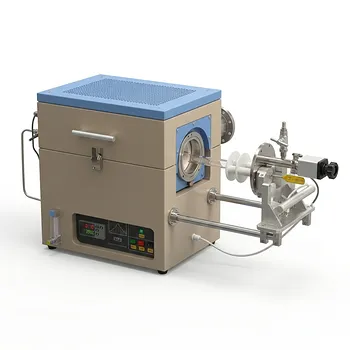
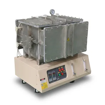
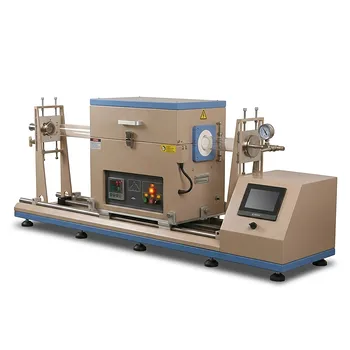
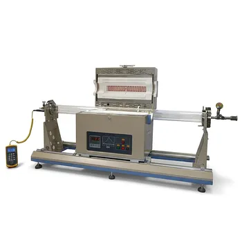
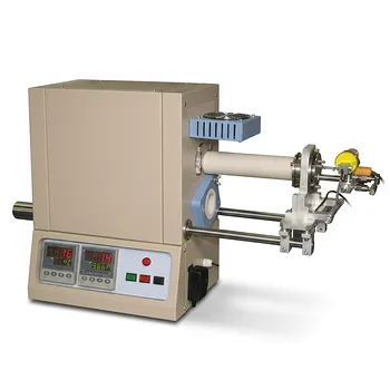
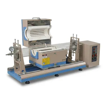
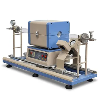
- Rapid Thermal Processing Furnace 1100C Atmosphere Controlled Bottom Loading RTP System for Wafer Annealing and Catalysis Research
- Rapid Thermal Processing RTP Atmosphere Controlled Bottom Loading Furnace 1100C High Throughput 50C per Second Heating Rate
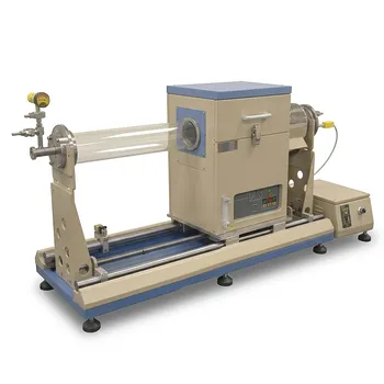
- 1200C Tube Furnace with Internal Magnetic Sample Sliding for Direct Vaporizing Deposition and Rapid Thermal Processing
- Compact Atmosphere Controlled Rapid Thermal Processing RTP Furnace with 4 Inch ID Quartz Tube 1100C
- Rapid Thermal Processing Atmosphere Controlled Bottom Loading Furnace 1100C with 50C Per Second Heating Rate for Wafer Annealing
People Also Ask
- What role does a SiC-coated graphite susceptor play in H2Se selenization? Boost RTP Thermal Uniformity & Film Purity.
- How does a Rapid Thermal Annealing (RTA) furnace differ from a traditional tube furnace? RTA vs. Tube for TiO2 Processing
- What are the functional advantages of an RTP system for surface deposition? Enhance Heterojunction Interface Integrity
- What are the advantages of RTPR for Pd1/PU catalyst synthesis? Achieve superior single-atom dispersion and stability.
- What role does a Rapid Thermal Processing (RTP) furnace play in Selenium recovery? Efficient Material Separation.
Tech Team · ThermUnits
Last updated on Jun 02, 2026
Related Products
Rapid Thermal Processing Furnace 1100C Atmosphere Controlled Bottom Loading RTP System for Wafer Annealing and Catalysis Research
Rapid Thermal Processing RTP Atmosphere Controlled Bottom Loading Furnace 1100C High Throughput 50C per Second Heating Rate
1200C Tube Furnace with Internal Magnetic Sample Sliding for Direct Vaporizing Deposition and Rapid Thermal Processing
Compact Atmosphere Controlled Rapid Thermal Processing RTP Furnace with 4 Inch ID Quartz Tube 1100C
Rapid Thermal Processing Atmosphere Controlled Bottom Loading Furnace 1100C with 50C Per Second Heating Rate for Wafer Annealing
950C Rapid Thermal Processing Furnace for 12 Inch Wafer CSS Coating with Rotating Substrate Holder
Two Zones CSS Furnace for Rapid Thermal Processing Thin Film Coating 3 Inch Diameter 650C
1500°C Atmosphere Controlled Rapid Heating Furnace for Material Science and Battery Powder Sintering
High Temperature Ultrafast Heating Pressing Furnace 2900C Max 100kgf Rapid Thermal Processing System
900 ºC Max Sliding RTP Tube Furnace with Rapid IR Heating and 4 Inch OD Quartz Tube
Ultrafast Thermal Pressing Furnace 2900C Max Temperature 200K per Second Heating Rate Vacuum Atmosphere Rapid Processing System
1200C Sliding Tube Furnace for Rapid Thermal Processing and CVD Graphene Growth with 100mm OD Capacity
High Temperature 800C Rapid Thermal Processing Furnace with Rotating Sample Holder for Close Spaced Sublimation and Thin Film Solar Cell Research
Rapid Thermal Processing Sliding Tube Furnace with 4 Inch OD Quartz Tube and 900C IR Heating
High Temperature Cold Wall Vacuum Furnace for Advanced Material Sintering and Annealing 1600C Heating Area 200x200x300mm
1200C Max Sliding Tube Furnace with 80mm OD Quartz Tube and Vacuum Flanges for Rapid Thermal Processing Fast Heating and Cooling
High Temperature Tube Furnace 1500C with Sliding Flanges and 50mm OD for Rapid Thermal Processing Fast Heating and Cooling
1200C High Temperature 5 Inch Sliding Tube Furnace for Rapid Thermal Processing RTP and Wafer Annealing
Automated Sliding Tube Furnace for Fast Heating and Cooling 2 Inch OD 1100C Max