What are the technical advantages of LPCVD for tunneling oxide? Achieve High-Precision Uniformity and Quality
Updated 3 months ago
LPCVD systems are the industry standard for preparing tunneling oxide and polysilicon layers because they provide unmatched thickness uniformity and conformal step coverage. By operating in a low-pressure environment, these systems enable precise control over ultrathin films, such as 1.6 nm tunneling oxides, while minimizing impurities that could compromise the electrical performance of high-efficiency silicon solar cells.
Core Takeaway: LPCVD technology leverages reduced pressure to prioritize surface-level chemical reactions over gas-phase nucleation, resulting in dense, high-purity, and exceptionally uniform thin films across large-scale production batches.
Superior Film Quality and Uniformity
Precision Control at the Nanoscale
LPCVD systems allow for the precise control of tunneling oxide layer thickness, often targeting a specific 1.6 nm threshold. This level of accuracy is critical for ensuring consistent quantum tunneling effects across the entire surface of a semiconductor or solar cell.
Exceptional Step Coverage and Density
The process produces a dense film structure with superior conformal coverage, even on complex geometries or high-aspect-ratio features. This ensure that the 200 nm polycrystalline silicon (poly-Si) layer deposited over the oxide maintains a high-quality interface necessary for efficient carrier transport.
Enhanced Gas-Phase Diffusion
Operating at reduced pressures (typically 0.1 to 100 Pa) increases the mean free path of gas molecules. This allows reactant gases to diffuse more effectively, ensuring that the film grows at a consistent rate across the entire wafer surface, regardless of its position in the furnace.
Enhanced Purity and Structural Integrity
Minimizing Gas-Phase Contamination
The low-pressure environment significantly reduces homogeneous gas-phase nucleation, which is the formation of unwanted particles in the air rather than on the substrate. By favoring heterogeneous surface reactions, LPCVD minimizes impurities and defects that could lead to signal leakage or poor passivation.
Managing Internal Stress
High-precision gas flow control allows manufacturers to adjust the chemical composition of the film, such as achieving a silicon-rich state in silicon nitride films. This capability is used to reach a low residual tensile stress (approximately 100 MPa), preventing the thin membranes from fracturing or degrading during subsequent manufacturing steps.
Electrical Insulation and Thermal Stability
LPCVD-deposited silicon dioxide (SiO2) serves as a highly dense insulating dielectric. This density is vital for preventing signal leakage in harsh environments and ensuring that the electrical integrity of the passivation contact remains stable under high-temperature conditions.
Understanding the Trade-offs
The Wrap-Around Effect
Unlike PECVD (Plasma Enhanced Chemical Vapor Deposition), LPCVD is typically a batch process that results in double-sided deposition. This "wrap-around" effect can deposit unwanted material on the rear side of the wafer, which may require additional etching steps to remove.
Thermal Stress on Equipment
LPCVD often requires high operating temperatures, sometimes exceeding 500°C for silicon and much higher for other materials. This intense heat can cause physical damage to quartz furnace tubes and wafer carriers over time, leading to higher maintenance costs compared to lower-temperature plasma-based systems.
Deposition Speed vs. Quality
While LPCVD provides superior film density and uniformity, it can be slower than atmospheric or plasma-enhanced processes. Achieving the highest level of film purity and structural integrity requires a careful balance of temperature and pressure, which may limit overall throughput in some high-volume scenarios.
How to Apply This to Your Project
When deciding whether to implement LPCVD for your thin-film deposition needs, consider your primary performance metrics and structural requirements.
- If your primary focus is ultrathin layer precision: Choose LPCVD for its ability to maintain 1.6 nm oxide layers with extreme uniformity across large batches.
- If your primary focus is complex surface geometry: Utilize LPCVD's high mean free path to ensure conformal step coverage on high-aspect-ratio features where other methods might fail.
- If your primary focus is minimizing electrical leakage: Opt for the high-density film structures produced by high-temperature LPCVD to ensure maximum insulation and carrier transport efficiency.
- If your primary focus is single-sided deposition: Consider PECVD instead, as it avoids the wrap-around effect and reduces the need for back-side etching.
LPCVD remains the definitive choice for applications where the integrity of the interface and the precision of the atomic-scale layer are the most critical factors for success.
Summary Table:
| Key Feature | Impact on Performance | Primary Advantage |
|---|---|---|
| Low-Pressure Control | Increases gas mean free path | Exceptional thickness uniformity across large batches |
| Surface-Level Reaction | Minimizes gas-phase nucleation | High-purity films with significantly fewer defects |
| Nanoscale Precision | Precise 1.6 nm oxide growth | Consistent quantum tunneling for solar and semi-conductors |
| Dense Film Structure | Enhanced insulating properties | Superior electrical stability and reduced signal leakage |
Elevate Your Thin-Film Research with THERMUNITS
As a leading manufacturer of high-temperature laboratory equipment, THERMUNITS provides the precision and reliability essential for advanced material science and industrial R&D. Our comprehensive range of thermal processing solutions includes LPCVD, CVD, and PECVD systems specifically designed to meet the rigorous demands of tunneling oxide and polysilicon layer preparation.
From Muffle, Vacuum, and Tube furnaces to specialized Hot Press, Rotary, and Vacuum Induction Melting (VIM) furnaces, we deliver the tools you need to achieve superior film quality and thermal stability.
Ready to optimize your lab’s efficiency and thin-film performance?
Contact our technical experts today to discuss your custom thermal processing needs and discover how our equipment can drive your innovation forward!
References
- Qinqin Wang, Jianning Ding. Effects on Metallization of n+-Poly-Si Layer for N-Type Tunnel Oxide Passivated Contact Solar Cells. DOI: 10.3390/ma17112747
Mentioned Products
- Radio Frequency Plasma Enhanced Chemical Vapor Deposition RF PECVD System for Laboratory and Industrial Thin Film Growth
- Chemical Vapor Deposition CVD System Slide PECVD Tube Furnace with Liquid Gasifier PECVD Machine
- 915MHz MPCVD Diamond Machine Microwave Plasma Chemical Vapor Deposition System Reactor
- Cylindrical Resonator MPCVD Machine System for Microwave Plasma Chemical Vapor Deposition and Lab Diamond Growth
- Split Chamber CVD Tube Furnace with Vacuum Station Chemical Vapor Deposition System Machine
People Also Ask
- What are the advantages of PECVD systems for nano flame retardant films? Protect Heat-Sensitive Polymers with Precision
- How does PECVD differ from conventional thermal CVD? Key Advantages of Low-Temperature Deposition for R&D
- What is the role of CVD/PECVD systems in the research of optoelectronic materials and functional coatings? Expert Guide
- What are the benefits of using PECVD for optical and photonic coatings? Achieve High-Precision Thin-Film Deposition
- How do RF frequency and power settings influence the characteristics of a PECVD process? Master Quality & Efficiency

Tech Team · ThermUnits
Last updated on Jun 02, 2026
Related Products
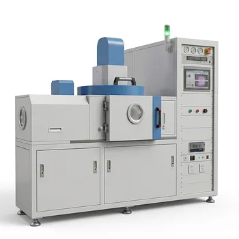
Radio Frequency Plasma Enhanced Chemical Vapor Deposition RF PECVD System for Laboratory and Industrial Thin Film Growth
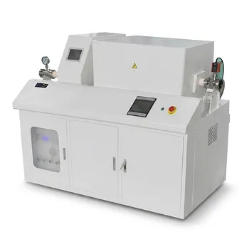
Chemical Vapor Deposition CVD System Slide PECVD Tube Furnace with Liquid Gasifier PECVD Machine
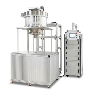
915MHz MPCVD Diamond Machine Microwave Plasma Chemical Vapor Deposition System Reactor
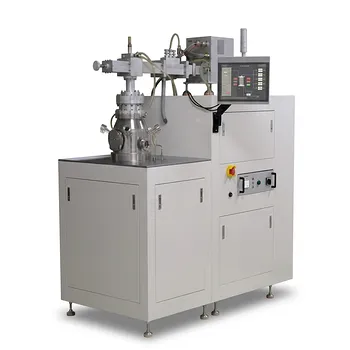
Cylindrical Resonator MPCVD Machine System for Microwave Plasma Chemical Vapor Deposition and Lab Diamond Growth
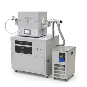
Split Chamber CVD Tube Furnace with Vacuum Station Chemical Vapor Deposition System Machine
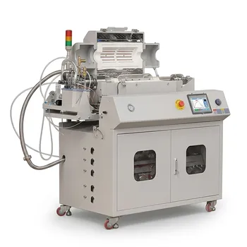
Versatile Chemical Vapor Deposition Tube Furnace System for Advanced Material Research and Industrial Coating Processes
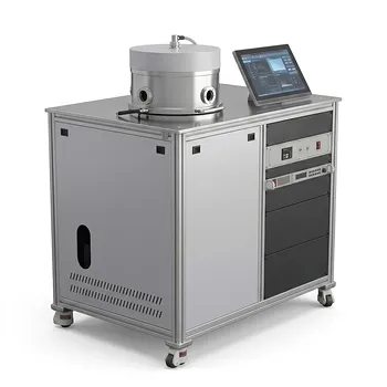
Inclined Rotary Plasma Enhanced Chemical Vapor Deposition PECVD System for Thin Film Deposition and Nanomaterial Synthesis
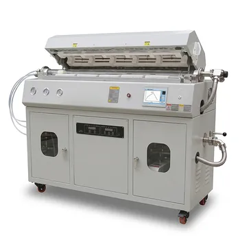
Multi Heating Zones CVD Tube Furnace System for Precision Chemical Vapor Deposition and Advanced Material Synthesis
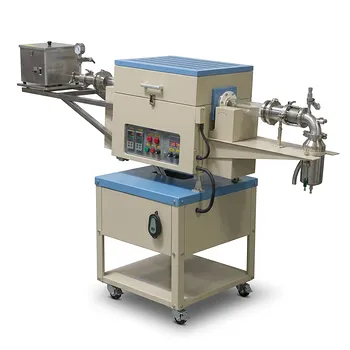
Two Zone Rotary CVD Furnace with Automatic Feeding and Receiving System for Powder Processing
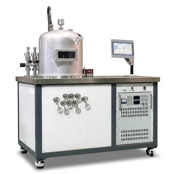
HFCVD Machine System for Nano Diamond Coating on Drawing Dies and Industrial Tools
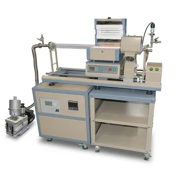
1200C Max Compact Auto-Sliding PECVD Furnace with 2 Inch Tube and Vacuum Pump
1000C Mini Tube Furnace with 20mm Quartz Tube and Vacuum Flanges for Material Science Research and Controlled Atmosphere Small Sample Processing
Dual Tube 100mm 80mm CVD Sliding Furnace with 4 Channel Gas Mixing and Vacuum System
1200C Sliding Internal Crucible Tube Furnace for Controlled Atmosphere Thin Film Deposition and Material Sublimation Research
5 Inch Rotary Tube Furnace with Automatic Feeding and Receiving System 1200C Three Zone CVD Powder Processing
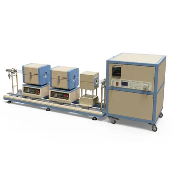
1200C Dual Sliding Tube Furnace with Dual Tubes and Flanges for PECVD Processes
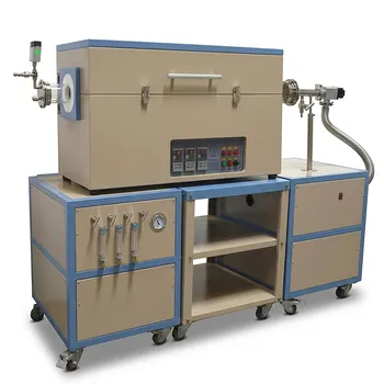
Three Zone Quartz Tube Furnace with 3 Channel Gas Mixer Vacuum Pump and Anti Corrosive Vacuum Gauge
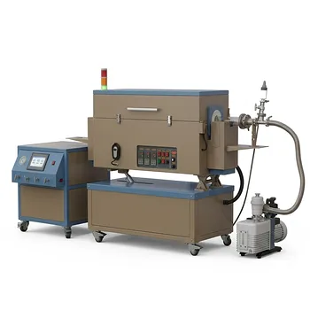
5 Inch Three Zone Rotary Tube Furnace with Integrated Gas Delivery System and 1200C Capability for Advanced Material CVD Processing
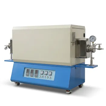
Three Temperature Zone High Temperature Vacuum Tube Furnace for CVD and Material Sintering