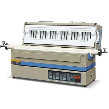
What role does a tube furnace play in a-Si crystallization & P-doping? Optimize High-Efficiency Solar Cell Production
Updated 3 months ago
The high-temperature tube diffusion furnace is the central engine for creating high-quality n+ passivated contacts in silicon solar cells. It provides the precise thermal energy—typically maintained at approximately 850 °C—required to trigger the phase transformation of deposited amorphous silicon (a-Si) into a stable polycrystalline silicon (poly-Si) structure. Simultaneously, the furnace acts as a chemical reactor that introduces phosphorus sources to achieve synchronized doping, ensuring the dopant reaches the required depth and concentration for optimal electrical performance.
Core Takeaway: The furnace serves as a dual-purpose thermal and chemical environment that transforms the physical structure of silicon films while precisely controlling their electrical conductivity through synchronized phosphorus diffusion.
The Catalyst for Solid-Phase Crystallization (SPC)
Facilitating Phase Transformation
The primary role of the furnace is to provide the stable thermal field necessary for solid-phase crystallization. By maintaining high temperatures (ranging from 850 °C to 920 °C), the furnace enables amorphous silicon layers to reorganize their atomic structure into a polycrystalline state.
Enhancing Mechanical and Chemical Stability
High-temperature environments promote the reorganization of chemical bonds within auxiliary layers, such as silicon carbide. This process breaks weaker Si-H and C-H bonds to form stable Si-C bonds, which significantly improves the film's mechanical strength and its effectiveness as a diffusion barrier.
Ensuring Structural Uniformity
The "tube" design of the furnace is critical for creating a constant temperature zone. This consistency ensures that the nucleation and growth kinetics of the silicon crystals are uniform across the entire surface of the wafer, preventing localized defects.
Precision Synchronized Phosphorus Doping
Introduction of Dopant Sources
During the crystallization process, the furnace introduces a precise mixture of phosphorus oxychloride (POCl3), oxygen, and nitrogen. This allows for synchronized doping, where phosphorus atoms are integrated into the silicon lattice at the same time the film is crystallizing.
Controlling the Doping Profile
The furnace’s precisely controlled thermal field determines the depth distribution of phosphorus atoms within the polycrystalline layer. This control is vital for achieving the desired sheet resistance, which directly influences how efficiently the final device transports electrical carriers.
Activation of Dopant Atoms
Beyond just placing phosphorus atoms into the film, the high-temperature environment activates them. This ensures the dopants are properly positioned within the silicon crystal lattice to contribute to the material's conductivity and the formation of critical p-n or high-low junctions.
Managing the Passivation Interface
Growth of Ultra-Thin Oxide Layers
High-precision tube furnaces are also utilized for thermal oxidation to grow ultra-thin silicon oxide (SiOx) layers, often around 1.7 nm thick. These layers are fundamental to tunneling passivated contact structures, providing the necessary carrier selectivity for high-efficiency cells.
Balancing Chemical and Field-Effect Passivation
By regulating annealing temperatures and "soaking" times, the furnace optimizes the active concentration of dopants at the interface. This balance maintains a low interface state density, which reduces electron recombination and improves the overall voltage of the solar cell.
Understanding the Trade-offs and Challenges
Thermal Budget vs. Material Degradation
While high temperatures are necessary for crystallization and doping activation, excessive thermal exposure can lead to the unwanted diffusion of impurities. Managing the "thermal budget" is a constant challenge to ensure performance gains in the poly-Si layer do not come at the cost of degrading the underlying silicon wafer.
Uniformity vs. Throughput
In an industrial setting, achieving a perfectly uniform thermal and gas flow field across a large batch of wafers is difficult. Minor fluctuations in the POCl3 gas flow or temperature gradients within the tube can lead to variations in sheet resistance, affecting the consistency of the final product.
How to Apply This to Your Project
Making the Right Choice for Your Goal
- If your primary focus is maximizing carrier transport: Prioritize precise control of the $POCl_3$ flow and soaking time to achieve a deep, high-concentration phosphorus profile with low sheet resistance.
- If your primary focus is enhancing surface passivation: Focus on the furnace's ability to grow a uniform, high-density ultra-thin $SiO_x$ layer at lower, more controlled oxidation temperatures.
- If your primary focus is structural integrity of the film: Utilize higher temperature ranges (near 920 °C) to ensure the complete breakage of hydrogen bonds and the formation of stable $Si-C$ or $Si-Si$ lattice structures.
The high-temperature tube diffusion furnace remains the definitive tool for synthesizing the complex structural and electrical requirements of modern silicon thin-film architectures.
Summary Table:
| Process Step | Primary Function | Key Performance Impact |
|---|---|---|
| Solid-Phase Crystallization | Converts a-Si to stable poly-Si lattice | Enhances structural and chemical stability |
| Synchronized P-Doping | Introduces phosphorus via POCl3 | Controls sheet resistance and conductivity |
| Interface Passivation | Grows ultra-thin (~1.7nm) SiOx layers | Reduces electron recombination rates |
| Thermal Activation | Positions dopant atoms in the lattice | Ensures efficient electrical carrier transport |
Elevate Your Material Science Research with THERMUNITS
As a leading manufacturer of high-temperature laboratory equipment, THERMUNITS provides the precision thermal solutions required for advanced semiconductor and photovoltaic R&D. Our high-performance Tube, Vacuum, Atmosphere, and Hot Press furnaces are engineered to deliver the uniform thermal fields and precise gas control necessary for successful crystallization and diffusion processes.
From CVD/PECVD systems to industrial-grade rotary kilns, we empower researchers and manufacturers to achieve superior material properties. Contact our technical experts today to discuss your specific heat treatment requirements and see how our expertise can accelerate your project.
References
- Qinqin Wang, Jianning Ding. Effects on Metallization of n+-Poly-Si Layer for N-Type Tunnel Oxide Passivated Contact Solar Cells. DOI: 10.3390/ma17112747
Mentioned Products
- High Temperature Dual Zone Rotating Tube Furnace 1500C Silicon Carbide Heating for Advanced Material Synthesis
- High Temperature 1700C Vertical Split Tube Furnace for Material Quenching and Single Crystal Growth
- High Temperature Tube Furnace 1500C with Sliding Flanges and 50mm OD for Rapid Thermal Processing Fast Heating and Cooling
- High Temperature 1700C Vertical Tube Furnace for Powder Spherification and Material Sintering
- High Temperature Vertical Hybrid Furnace with Alumina Tube and SiC Heating for SOFC Coin Cell Testing and Atmosphere Processing
People Also Ask
- What is the function of CVD furnaces in graphene prep? Enhancing Photodetector Charge Transport
- Why use CVD and a tube furnace for Pd3P0.95/NC catalyst phosphidation? Ensure high phase purity and performance.
- CVD Tube Furnace Advantages for Pd-P Catalyst Durability: Precision Control for 40,000+ Cycles
- How does a rotary tube furnace improve the processing of granular materials? Enhance Uniformity and Reaction Kinetics
- How does a Chemical Vapor Deposition (CVD) tube furnace facilitate synchronized nitridation? Precision Nano-Engineering.

Tech Team · ThermUnits
Last updated on Jun 02, 2026
Related Products
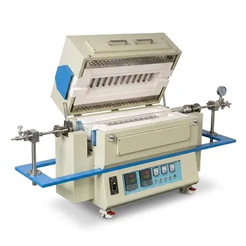
High Temperature Dual Zone Rotating Tube Furnace 1500C Silicon Carbide Heating for Advanced Material Synthesis
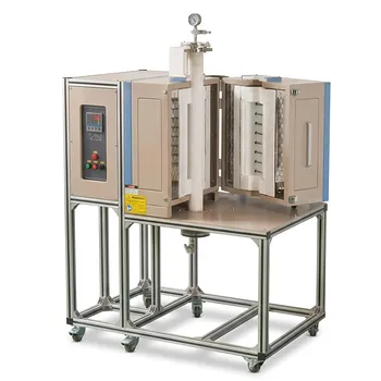
High Temperature 1700C Vertical Split Tube Furnace for Material Quenching and Single Crystal Growth
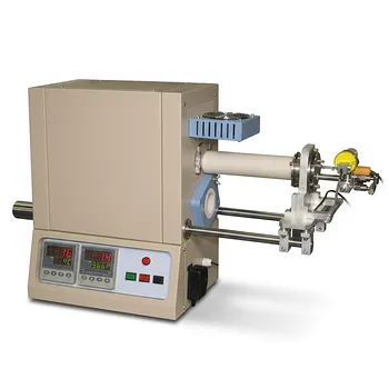
High Temperature Tube Furnace 1500C with Sliding Flanges and 50mm OD for Rapid Thermal Processing Fast Heating and Cooling
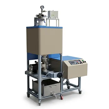
High Temperature 1700C Vertical Tube Furnace for Powder Spherification and Material Sintering
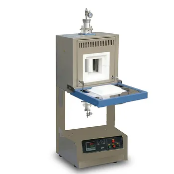
High Temperature Vertical Hybrid Furnace with Alumina Tube and SiC Heating for SOFC Coin Cell Testing and Atmosphere Processing
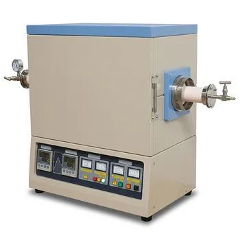
High Temperature 1700C Dual Zone Tube Furnace for Material Science and Industrial Chemical Vapor Deposition Research
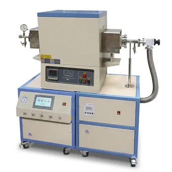
High Temperature 1700C Tube Furnace with High Vacuum Turbomolecular Pump System and Multi Channel Mass Flow Controller Gas Mixer
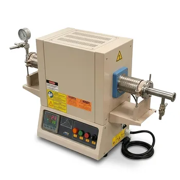
Compact High Temperature 1600C Tube Furnace with 50mm Alumina Tube and Vacuum Flanges for Material Sintering
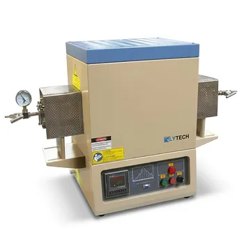
1800C High Temperature Compact Vacuum Tube Furnace with 60mm OD Alumina Tube and Kanthal MoSi2 Heating Elements
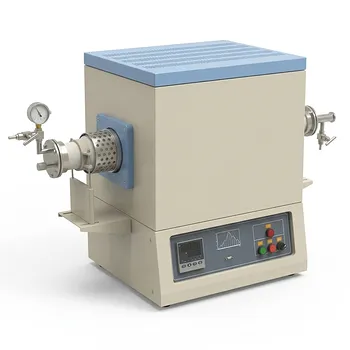
1750°C High Temperature Benchtop Vacuum Atmosphere Tube Furnace with Kanthal Super 1800 Heating Elements and 60mm Alumina Processing Tube
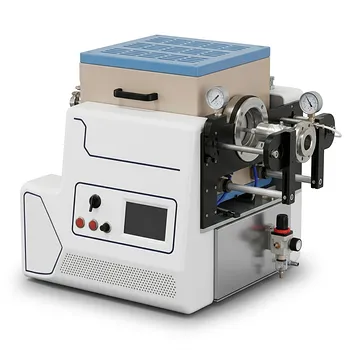
High Temperature Automated 5 Inch Tube Furnace for Autonomous Material Research and Advanced Laboratory R&D
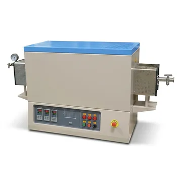
Three Zone Alumina Tube Furnace with Vacuum Flanges High Temperature 1700C Thermal Gradient CVD System
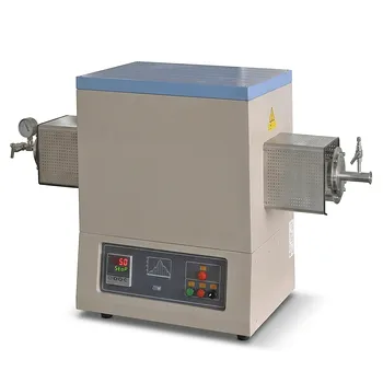
High Temperature 1700C Tube Furnace with 4 Inch OD Alumina Tube and Vacuum Sealing Flanges
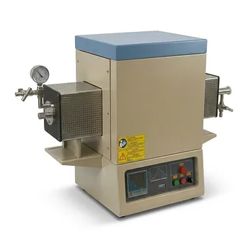
High Temperature 1700C Benchtop Tube Furnace with 5 Inch Heating Zone High Purity Alumina Tube and Vacuum Sealing Flanges
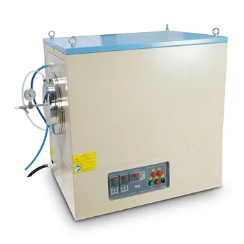
Dual Zone Tube Furnace 1100C with 11 Inch Quartz Tube and Vacuum Flanges for 8 Inch Wafer Processing
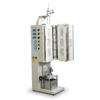
High Temperature Dual Zone Tube Furnace for Material Science Research and Professional Thermal Processing
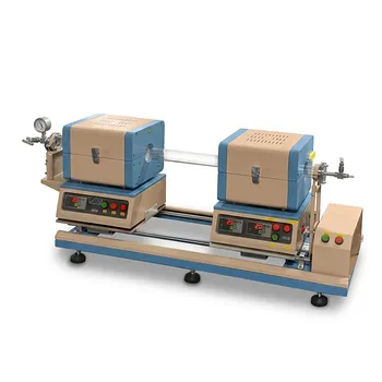
High Temperature 1200C Automatic Sliding Dual Zone Tube Furnace for 2D Transition Metal Dichalcogenides Growth and Material Sublimation Research
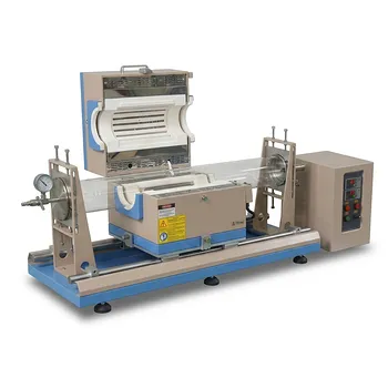
1200C High Temperature 5 Inch Sliding Tube Furnace for Rapid Thermal Processing RTP and Wafer Annealing
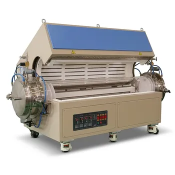
1200C Max Four Zone Split Tube Furnace with Optional Large Diameter Quartz Tubes