Why is high-temperature annealing in a quartz tube furnace done after HfO2 deposition? Unlock peak film performance.
Updated 3 months ago
High-temperature annealing is the essential activation step for hafnium oxide ($HfO_2$) thin films. It transforms the "as-deposited" layer into a functional electronic barrier by inducing chemical reorganization and optimizing the distribution of fixed charges. This process, typically performed between 350°C and 600°C, is required to reduce surface recombination and dramatically boost the minority carrier lifetime of the underlying silicon wafer.
Core Takeaway: Annealing in a quartz tube furnace facilitates the thermal diffusion and lattice rearrangement necessary to lower interface state density and activate the film's passivation properties. Without this post-deposition treatment, the thin film remains electronically "dormant" and lacks the structural integrity required for high-performance semiconductor applications.
Activating Passivation Performance
Enhancing Minority Carrier Lifetime
The primary goal of annealing $HfO_2$ is to "activate" its ability to protect the silicon surface. This activation significantly reduces the surface recombination rate, which allows charge carriers to survive longer within the wafer.
Optimizing Charge Distribution
During the heating process in an air atmosphere, the film undergoes a chemical reorganization. This process adjusts the fixed charge density within the layer, which is critical for creating the field-effect passivation required in modern solar cells and transistors.
Managing Interface State Density
The transition zone between the silicon and the hafnium oxide is often riddled with defects after initial deposition. Annealing provides the thermal energy to "heal" these defects, lowering the interface state density ($D_{it}$) and ensuring a smoother electronic transition.
Structural and Chemical Evolution
Elimination of Internal Stresses
Deposition methods like sputtering often leave the thin film in a state of high internal stress. The controlled environment of a quartz tube furnace allows atoms to reach their equilibrium positions, effectively neutralizing these stresses and preventing future film delamination.
Phase Transformation and Crystallinity
As-deposited films are frequently amorphous or poorly structured. High-temperature treatment provides the necessary energy for lattice rearrangement, often transitioning the material toward a more stable crystalline phase, such as the monoclinic phase, which enhances thermal and chemical stability.
Removal of Impurities and Precursors
In many deposition processes, residual organic binders or nitrogen-based precursors remain trapped in the film. Annealing at temperatures like 550°C to 800°C ensures these impurities are fully oxidized or outgassed, resulting in a high-purity metal oxide layer.
Understanding the Trade-offs
The Risk of Over-Annealing
While heat is necessary for activation, excessive temperatures can lead to unwanted grain growth. Large grain boundaries can act as leakage paths for electrical current, potentially degrading the insulating properties of the $HfO_2$ layer.
Thermal Budget Constraints
Every semiconductor device has a "thermal budget," or the total amount of heat it can withstand before existing junctions begin to diffuse or degrade. Engineers must balance the high temperatures required for $HfO_2$ crystallization (often above 600°C) against the sensitivity of the underlying substrate.
Atmospheric Sensitivity
The choice of atmosphere in the tube furnace—whether air, nitrogen, or vacuum—radically changes the film's final properties. For instance, annealing in air is vital for stoichiometry and oxygen vacancy control, but it can also lead to the unwanted growth of a thick, low-k interfacial silicon dioxide ($SiO_2$) layer.
How to Apply This to Your Project
Recommendations for Process Optimization
- If your primary focus is Maximum Passivation: Use a moderate temperature range (350°C–450°C) in an air or forming gas atmosphere to optimize the interface without inducing heavy crystallization.
- If your primary focus is Structural Stability: Aim for higher temperatures (above 600°C) to ensure a transition to a crystalline phase, which provides better resistance to subsequent high-temperature manufacturing steps.
- If your primary focus is Leakage Reduction: Keep annealing times short and temperatures controlled to prevent the formation of large grain boundaries that facilitate current leakage.
Properly executed annealing turns a simple deposited layer into a high-performance electronic component by balancing chemical activation with structural refinement.
Summary Table:
| Aspect | Benefit of Annealing | Final Outcome |
|---|---|---|
| Passivation | Reduces surface recombination | Boosts minority carrier lifetime |
| Structural | Induces lattice rearrangement | Transitions to stable crystalline phase |
| Interface | Lowers state density ($D_{it}$) | Ensures smoother electronic transition |
| Purity | Oxidizes/outgasses impurities | High-purity, stable metal oxide layer |
| Stress | Neutralizes internal stresses | Prevents film delamination and cracking |
Precision Thermal Solutions for Semiconductor R&D
Achieving perfect $HfO_2$ passivation requires the exact temperature and atmospheric control that only high-quality laboratory equipment can provide. THERMUNITS is a leading manufacturer of high-temperature laboratory equipment for material science and industrial R&D.
We offer a comprehensive range of thermal processing solutions tailored for thin-film research, including:
- Tube & Vacuum Furnaces: Ideal for precise $HfO_2$ annealing and CVD/PECVD applications.
- Advanced Systems: Atmosphere, Muffle, Rotary, and Hot Press furnaces, plus Vacuum Induction Melting (VIM).
- Specialized Tools: Dental furnaces, electric rotary kilns, and high-quality Thermal Elements.
Empower your material research with uniform heating and reliable performance. Contact THERMUNITS today to optimize your lab’s heat treatment workflow!
References
- Sophie L. Pain, John D. Murphy. Atomic Layer Deposition of Hafnium Oxide Passivating Layers on Silicon: Impact of Precursor Selection. DOI: 10.1002/pssr.202400202
Mentioned Products
- Dual Zone Quartz Tube Furnace with 80mm Diameter 1200C Max Temperature 3 Channel Gas Mixer and Vacuum Pump System
- 1100°C High Temperature Quartz Chamber Furnace 8 Inch OD with 7.6 Liter Capacity and Vacuum Atmosphere Capability
- Compact Vertical Split Quartz Tube Furnace with Stainless Steel Vacuum Flanges for Rapid Thermal Quenching and Controlled Atmosphere Material Processing
- 1100°C Large Diameter Quartz Tube Furnace with 24 Inch Heating Zone and Water Cooled Flanges
- 1200°C 5 Inch Vertical Quartz Tube Furnace with Stainless Steel Vacuum Flanges
People Also Ask
- How do dual-zone quartz tube furnaces achieve controllable material preparation? Optimize Perovskite VD Processes
- What are the technical advantages of using a dual-zone tube furnace for growing large PdCoO2 crystals via CVT? Expert Tips
- Purpose of the reverse gradient step in CVT growth? Master Crystal Purity with Dual-Zone Furnaces
- Why is it necessary to place MoS2 devices in a dual-zone tube furnace for annealing? Optimize Lattice Repair & Doping
- Why is a dual-zone tube furnace necessary for ReO3-doped Cu2Te CVD? Essential for precise precursor synchronization.

Tech Team · ThermUnits
Last updated on Jun 03, 2026
Related Products
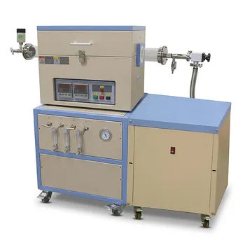
Dual Zone Quartz Tube Furnace with 80mm Diameter 1200C Max Temperature 3 Channel Gas Mixer and Vacuum Pump System
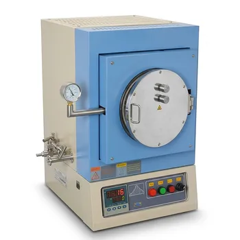
1100°C High Temperature Quartz Chamber Furnace 8 Inch OD with 7.6 Liter Capacity and Vacuum Atmosphere Capability
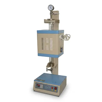
Compact Vertical Split Quartz Tube Furnace with Stainless Steel Vacuum Flanges for Rapid Thermal Quenching and Controlled Atmosphere Material Processing
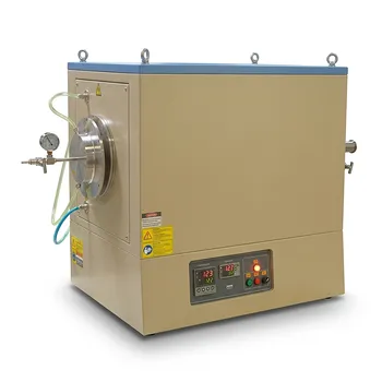
1100°C Large Diameter Quartz Tube Furnace with 24 Inch Heating Zone and Water Cooled Flanges
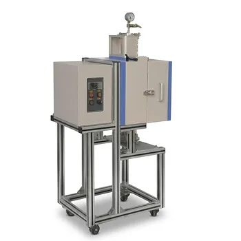
1200°C 5 Inch Vertical Quartz Tube Furnace with Stainless Steel Vacuum Flanges
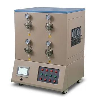
High Throughput 1200C Four Channel Tube Furnace with 3 Inch Quartz Tubes for Multi Zone Annealing and Material Research
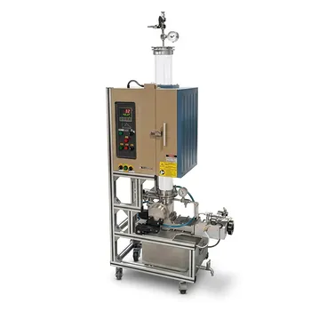
1200C High Temperature Atmosphere Controlled Vertical Quenching Tube Furnace with 4 Inch Quartz Tube
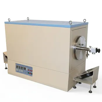
1100°C Three Zone Tube Furnace with 8.5 to 11 Inch OD Quartz Tube and Vacuum Flanges for Large Wafer Processing
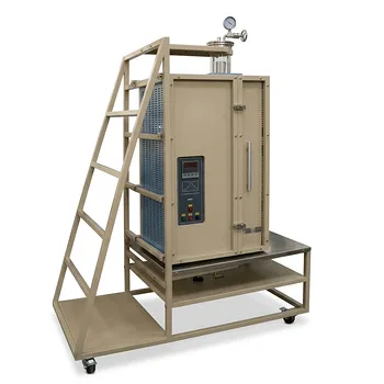
Split Vertical Tube Furnace with 1200C Quartz Tube and Stainless Steel Vacuum Flanges for Rapid Thermal Processing
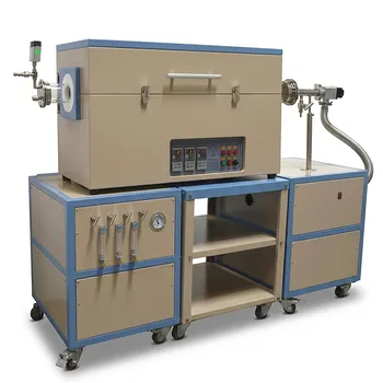
Three Zone Quartz Tube Furnace with 3 Channel Gas Mixer Vacuum Pump and Anti Corrosive Vacuum Gauge
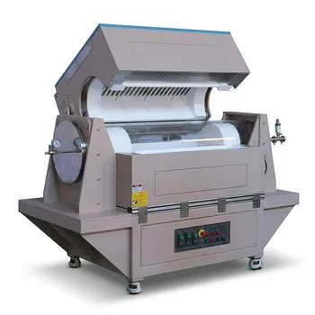
Three Zone Tube Furnace with 11 Inch or 15 Inch Quartz Tube and Hinged Flanges for Vacuum Atmosphere Heat Treatment
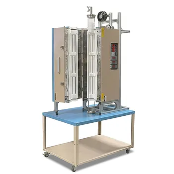
1200C Three Zone Split Vertical Tube Furnace 4 Inch Quartz Tube Stainless Steel Vacuum Flanges
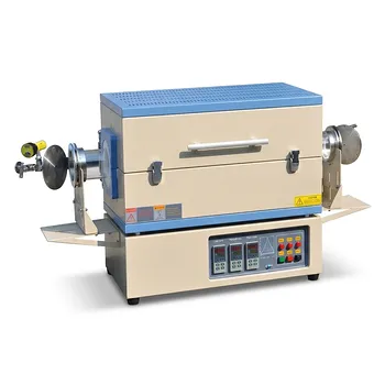
Three Zone Tube Furnace with 24 Inch Heating Length and Hinged Flange Quartz Tube System
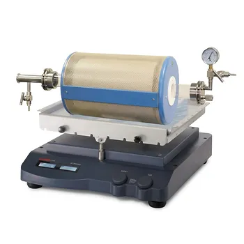
High Temperature Rocking Tube Furnace with Quartz Tube and Vacuum Flange for Materials Synthesis
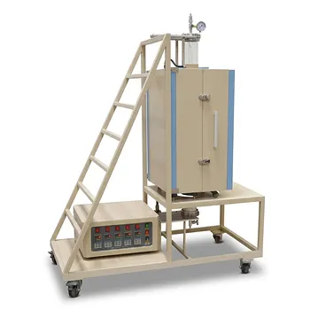
Five Zone Split Vertical Tube Furnace 1200C Max with 4 Inch Quartz Tube and Stainless Steel Vacuum Flanges
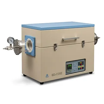
Single Zone Tube Furnace 5 Inch Quartz Tube 36 Inch Heating Zone Vacuum Flanges
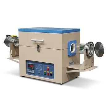
High Temperature 1200C Split Tube Furnace with Hinged Vacuum Flanges and 4 Inch Quartz Tube for Laboratory Research
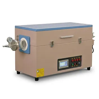
1200C Four Zone Split Tube Furnace with Touch Screen Control and High Purity Quartz Tube and Vacuum Sealing Flanges
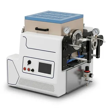
High Temperature Automated 5 Inch Tube Furnace for Autonomous Material Research and Advanced Laboratory R&D