What are the primary applications for PECVD in semiconductor manufacturing? Essential Thin-Film Fabrication Guide
Updated 5 months ago
Plasma-Enhanced Chemical Vapor Deposition (PECVD) is a critical fabrication process used to deposit thin films of insulating, semiconducting, or protective materials at significantly lower temperatures than standard CVD. In semiconductor manufacturing, its primary applications include the creation of interlayer dielectrics (ILD), passivation layers, etch-stops, and critical components for advanced 2.5D and 3D packaging.
PECVD is the industry standard for depositing high-quality thin films without exceeding the thermal budgets of sensitive substrates or metal interconnects. Its ability to tune film properties like stress and composition makes it indispensable for both logic device scaling and advanced heterogeneous integration.
Primary Applications in Logic and Memory Fabrication
Interlayer and Inter-metal Dielectrics (ILD/IMD)
PECVD is used to deposit the insulating layers that separate different levels of electrical wiring within a chip. These dielectric layers are essential for preventing short circuits while maintaining low capacitance between metal lines. Because PECVD operates at low temperatures, it can deposit these films over aluminum or copper interconnects without melting or damaging them.
Passivation and Etch-Stop Layers
The process is vital for creating passivation layers, which serve as the final protective "skin" of the chip to block moisture and contaminants. Additionally, PECVD is used to deposit silicon nitride (SiNx) or silicon oxynitride (SiON) films that act as etch-stops. These layers provide a precise termination point during chemical-mechanical planarization (CMP) or plasma etching processes.
Gate Dielectrics and Sidewall Spacers
In the front-end-of-line (FEOL) stages, PECVD helps form gate dielectrics and sidewall spacers. These structures are fundamental to the operation of transistors, providing electrical isolation and defining the physical dimensions of the transistor gate. The high degree of film conformality ensures that these features are uniform even across complex, three-dimensional transistor architectures.
Advanced Packaging and Emerging Technologies
2.5D and 3D Packaging Integration
As the industry moves toward high-performance computing and AI chips, PECVD has become critical for Through-Silicon Via (TSV) passivation. It provides the necessary insulation for vertical electrical connections that pass through the silicon wafer. Furthermore, it is used for hybrid bonding insulation, enabling the dense stacking of multiple chips in a single package.
Thin-Film Transistors (TFT) and MEMS
In the display industry, PECVD is the primary method for depositing amorphous silicon (a-Si) and dielectric layers for Thin-Film Transistors (TFTs). It is also used in Micro-Electro-Mechanical Systems (MEMS) to create structural and sacrificial layers. The ability to deposit these films over large areas with high uniformity makes the technology ideal for flat-panel displays and sensor manufacturing.
Doping Sources and Contact Formation
Advanced processes use PECVD to deposit phosphorus-doped amorphous silicon (a-Si:P) onto polycrystalline silicon. This layer acts as a controlled doping source, allowing atoms to diffuse into the underlying silicon during later annealing steps. This provides engineers with nanometer-scale precision over the conductivity and carrier concentration of device contacts.
Understanding the Trade-offs
The Challenge of Film Purity
While PECVD offers lower operating temperatures, the resulting films may contain higher levels of impurities, such as hydrogen, compared to high-temperature thermal CVD. This can lead to outgassing during subsequent high-temperature steps or impact the electrical stability of the film. Engineers must carefully balance the chemical precursors to minimize these effects.
Plasma-Induced Damage
The very plasma that enables low-temperature reactions can occasionally damage delicate gate oxides or surface structures through ion bombardment or charging effects. This requires precise control of the RF power and frequency within the PECVD chamber. Modern systems often use dual-frequency sources to balance deposition speed with the physical integrity of the substrate.
Applying PECVD to Your Project Goals
Recommendations for Implementation
- If your primary focus is thermal-sensitive substrates: Use PECVD to deposit films below 400°C to protect existing metal layers and prevent dopant diffusion.
- If your primary focus is mechanical reliability: Utilize the tunable nature of PECVD plasma parameters to adjust the internal stress of the film, preventing wafer bowing or film cracking.
- If your primary focus is high-aspect-ratio features: Prioritize PECVD for TSV passivation and 3D structures where superior step coverage and conformality are non-negotiable.
Choosing the right PECVD parameters ensures that you can achieve high-volume manufacturing throughput without sacrificing the delicate electrical properties of modern semiconductor devices.
Summary Table:
| Application Category | Primary Function | Key Materials Used |
|---|---|---|
| Interlayer Dielectrics (ILD) | Electrical isolation between metal wiring levels | Low-k Dielectrics |
| Passivation Layers | Final protective coating against moisture/contaminants | Silicon Nitride (SiNx) |
| Etch-Stop Layers | Precise termination points for CMP or plasma etching | Silicon Oxynitride (SiON) |
| Advanced 3D Packaging | Insulation for Through-Silicon Vias (TSV) | High-conformality films |
| Display & MEMS | Formation of structural and sacrificial layers | Amorphous Silicon (a-Si) |
| Transistor Spacers | Defining gate dimensions and providing isolation | Gate Dielectrics |
Elevate Your Material Research with THERMUNITS
Are you looking to optimize your thin-film deposition or high-temperature heat treatment processes? THERMUNITS is a leading manufacturer of high-performance laboratory equipment designed for material science and industrial R&D.
We offer a comprehensive suite of thermal solutions, including:
- Advanced CVD/PECVD Systems for precision thin-film applications.
- Muffle, Vacuum, and Atmosphere Furnaces for diverse heat treatments.
- Tube, Rotary, and Hot Press Furnaces for specialized material synthesis.
- Dental Furnaces, Electric Rotary Kilns, and Vacuum Induction Melting (VIM) Furnaces.
Whether you are scaling logic devices or developing advanced 2.5D/3D packaging, our expert-grade equipment ensures the reliability and control your project demands.
Contact THERMUNITS Today to discuss your specific requirements and find the perfect thermal processing solution for your lab!
Mentioned Products
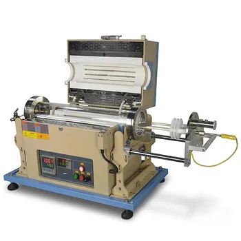
- Chemical Vapor Deposition CVD System Slide PECVD Tube Furnace with Liquid Gasifier PECVD Machine
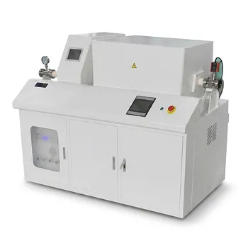
- Inclined Rotary Plasma Enhanced Chemical Vapor Deposition PECVD System for Thin Film Deposition and Nanomaterial Synthesis
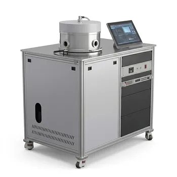
- Radio Frequency Plasma Enhanced Chemical Vapor Deposition RF PECVD System for Laboratory and Industrial Thin Film Growth
- 1200C Max Compact Auto-Sliding PECVD Furnace with 2 Inch Tube and Vacuum Pump
- 1200C Dual Sliding Tube Furnace with Dual Tubes and Flanges for PECVD Processes
People Also Ask
- What are the advantages of PECVD systems for nano flame retardant films? Protect Heat-Sensitive Polymers with Precision
- How does a sliding rail design benefit the CVD process within a furnace ventilation hood? Enhance Control & Quenching
- What is the role of CVD/PECVD systems in the research of optoelectronic materials and functional coatings? Expert Guide
- How does PECVD differ from conventional thermal CVD? Key Advantages of Low-Temperature Deposition for R&D
- What role do by-product desorption and evacuation play in CVD film quality? Key Factors for High-Purity Films

Tech Team · ThermUnits
Last updated on Apr 14, 2026
Related Products
Chemical Vapor Deposition CVD System Slide PECVD Tube Furnace with Liquid Gasifier PECVD Machine
Inclined Rotary Plasma Enhanced Chemical Vapor Deposition PECVD System for Thin Film Deposition and Nanomaterial Synthesis
Radio Frequency Plasma Enhanced Chemical Vapor Deposition RF PECVD System for Laboratory and Industrial Thin Film Growth
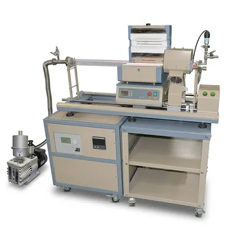
1200C Max Compact Auto-Sliding PECVD Furnace with 2 Inch Tube and Vacuum Pump
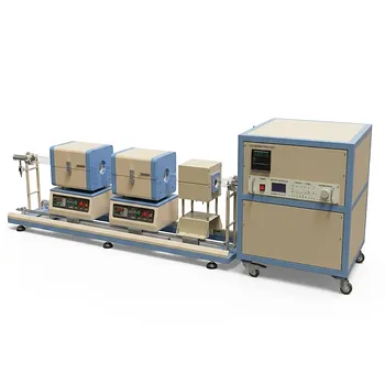
1200C Dual Sliding Tube Furnace with Dual Tubes and Flanges for PECVD Processes
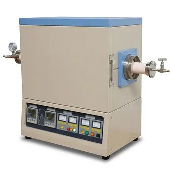
High Temperature 1700C Dual Zone Tube Furnace for Material Science and Industrial Chemical Vapor Deposition Research
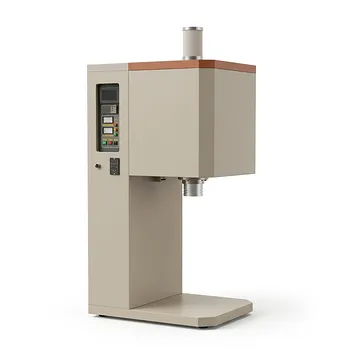
Vertical Openable Tube Furnace 0-1700c High Temperature Laboratory System for CVD and Vacuum Heat Treatment
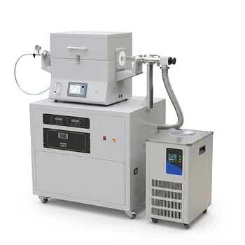
Split Chamber CVD Tube Furnace with Vacuum Station Chemical Vapor Deposition System Machine
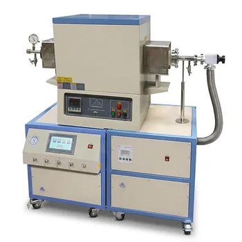
High Temperature 1700C Tube Furnace with High Vacuum Turbomolecular Pump System and Multi Channel Mass Flow Controller Gas Mixer
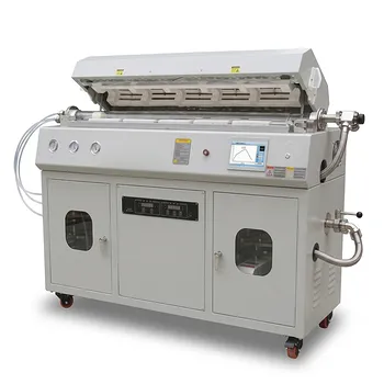
Multi Heating Zones CVD Tube Furnace System for Precision Chemical Vapor Deposition and Advanced Material Synthesis
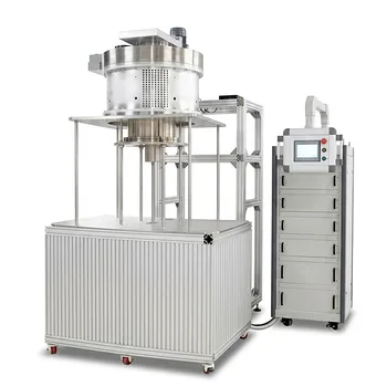
915MHz MPCVD Diamond Machine Microwave Plasma Chemical Vapor Deposition System Reactor
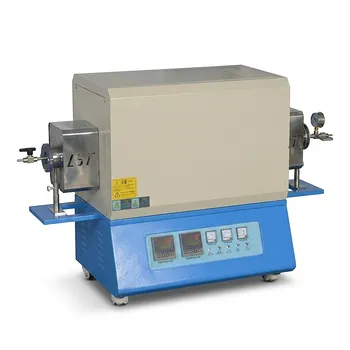
High Temperature Dual Zone Vacuum Tube Furnace for Material Research and CVD Processing
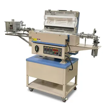
5 Inch Rotary Tube Furnace with Automatic Feeding and Receiving System 1200C Three Zone CVD Powder Processing
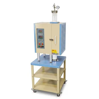
1100°C Dual Zone Split Vertical Tube Furnace with 4 Inch Quartz Tube and Vacuum Sealing Flanges
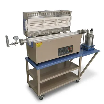
5 Inch Two Zone Rotary Tube Furnace 1100C for Powder CVD and Material Synthesis
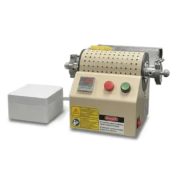
1000C Mini Tube Furnace with 20mm Quartz Tube and Vacuum Flanges for Material Science Research and Controlled Atmosphere Small Sample Processing
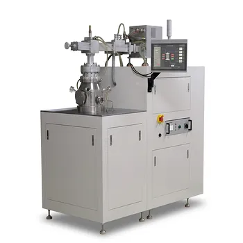
Cylindrical Resonator MPCVD Machine System for Microwave Plasma Chemical Vapor Deposition and Lab Diamond Growth
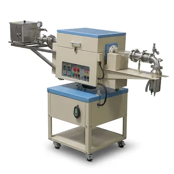
Two Zone Rotary CVD Furnace with Automatic Feeding and Receiving System for Powder Processing
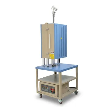
1200C Three Zone Vertical Tube Furnace with 2 Inch Quartz Tube and Vacuum Flanges