What are the technical advantages of using Low-Pressure Chemical Vapor Deposition (LPCVD)? Master Thin-Film Uniformity
Updated 5 months ago
Low-Pressure Chemical Vapor Deposition (LPCVD) is a sophisticated thin-film deposition technique that operates at reduced pressures, typically between 0.1 and 100 Pa. This specific environment increases the mean free path of gas molecules, significantly enhancing gas-phase diffusion and ensuring that chemical reactions occur primarily at the substrate surface rather than in the gas phase. These mechanics result in superior film uniformity, exceptional conformal coverage, and high-purity material layers.
Core Takeaway: LPCVD solves the challenge of depositing highly uniform and pure thin films across complex, high-aspect-ratio geometries. By optimizing molecular transport and minimizing gas-phase impurities, it provides a scalable solution for high-performance semiconductor and optoelectronic applications.
Optimized Gas Dynamics and Reaction Kinetics
Enhanced Molecular Diffusion
Operating at low pressures increases the mean free path of gas molecules, which is the average distance a particle travels before colliding with another. This allows reactant gases to diffuse more rapidly through the reaction chamber and into deep trenches.
This increased mobility ensures that reactants reach all areas of the substrate equally. It effectively eliminates the "shadowing" effects that often plague atmospheric pressure processes.
Minimization of Gas-Phase Nucleation
In higher-pressure environments, gas molecules often react with each other before reaching the substrate, creating unwanted particles or "dust." LPCVD’s low-pressure environment favors heterogeneous reactions, which occur directly on the wafer surface.
By suppressing these premature gas-phase reactions, the process maintains a cleaner environment. This leads to significantly higher film purity and fewer structural defects in the final layer.
Superior Film Quality and Precision
Conformal Coverage on Complex Geometries
LPCVD is the industry standard for conformal coverage, meaning the film follows the exact contours of the underlying topography. This is critical for modern 3D architectures, such as high-aspect-ratio trenches or nanocones.
Because the reaction is surface-controlled rather than supply-controlled, the film grows at a consistent rate on both horizontal and vertical surfaces. This ensures that the sidewalls of deep features are coated as thickly and reliably as the top surfaces.
Precise Thickness and Purity Control
The system allows for extreme precision, such as the deposition of tunneling oxide layers as thin as 1.6 nm. High-purity gases like silane (SiH4) or acetylene are used to achieve consistent chemical compositions.
In polysilicon deposition, this precision results in a uniform grain structure. This consistency is vital for maintaining a reliable electric field distribution and consistent device performance in mass production.
Industrial Scalability and Efficiency
High-Throughput Batch Processing
Unlike single-wafer systems that can suffer from low throughput at reduced temperatures, LPCVD vertical reactors are designed for batch processing. They can process between 50 and 100 large-sized wafers simultaneously.
This batch capability offsets the slower growth rates associated with lower thermal budgets. It allows manufacturers to meet high-volume production demands without sacrificing film quality.
Uniform Doping and Passivation
LPCVD ensures consistent film thickness across the entire surface of every wafer in a batch. This uniformity is essential for subsequent manufacturing steps, such as uniform doping diffusion.
Reliable passivation performance is a direct result of this consistency. It ensures that every device on a wafer meets the same high-performance electrical specifications.
Understanding the Trade-offs
Thermal Budget and Equipment Stress
LPCVD often requires medium to high temperatures (e.g., 530°C to 1,280°C) to facilitate surface reactions. These high temperatures can cause physical stress and damage to quartz furnace tubes and wafer carriers over time.
For temperature-sensitive substrates, this high thermal budget may be a limitation. In such cases, designers may have to look toward Plasma-Enhanced CVD (PECVD) as a lower-temperature alternative.
The Wrap-Around Effect
A common characteristic of LPCVD is the wrap-around effect, where the film deposits on both sides and the edges of the wafer. While this demonstrates excellent conformality, it may require additional cleaning or etching steps if single-sided deposition is required.
Systems like PECVD are often preferred when single-sided deposition is a primary requirement. However, for most structural layers, the uniformity of LPCVD outweighs the inconvenience of the wrap-around effect.
Making the Right Choice for Your Goal
To determine if LPCVD is the optimal process for your specific application, consider your primary technical objective:
- If your primary focus is Conformal Coating of 3D Structures: LPCVD is the definitive choice due to its superior surface-controlled reaction kinetics and ability to coat deep trenches uniformly.
- If your primary focus is High-Volume Production of Thin Oxides: Utilize batch LPCVD vertical reactors to maintain high throughput while achieving sub-2nm thickness precision.
- If your primary focus is Electrical Consistency in Gates: Choose LPCVD to ensure a uniform grain structure and consistent work function across polysilicon layers.
- If your primary focus is Single-Sided Deposition or Low Thermal Budget: Consider PECVD or other alternative methods to avoid the wrap-around effect and high-temperature stress on equipment.
By aligning the unique gas-phase dynamics of LPCVD with your structural requirements, you can achieve world-class film integrity and device reliability.
Summary Table:
| Feature | Technical Advantage | Key Industrial Outcome |
|---|---|---|
| Gas Dynamics | Increased Mean Free Path | Enhanced diffusion & superior film uniformity |
| Reaction Type | Surface-controlled Kinetics | Exceptional conformal coverage on 3D structures |
| Environment | Reduced Pressure (0.1-100 Pa) | Minimal gas-phase nucleation & high film purity |
| Scalability | Vertical Batch Processing | High-throughput for 50-100 wafers simultaneously |
| Precision | Controlled Deposition Rate | Accurate thickness control (e.g., <2nm oxide layers) |
Elevate Your Thin-Film Research with THERMUNITS
Precision in thermal processing is the backbone of material science innovation. THERMUNITS is a leading manufacturer of high-temperature laboratory equipment, providing state-of-the-art CVD/PECVD systems, Muffle, Vacuum, and Tube furnaces tailored for industrial R&D. Whether you are developing high-aspect-ratio semiconductors or advanced optoelectronics, our comprehensive range of thermal solutions—including electric rotary kilns and vacuum induction melting furnaces—ensures world-class results.
Ready to optimize your lab’s efficiency? Contact our technical experts today to discuss your specific heat treatment requirements!
Mentioned Products
- Radio Frequency Plasma Enhanced Chemical Vapor Deposition RF PECVD System for Laboratory and Industrial Thin Film Growth
- Chemical Vapor Deposition CVD System Slide PECVD Tube Furnace with Liquid Gasifier PECVD Machine
- Inclined Rotary Plasma Enhanced Chemical Vapor Deposition PECVD System for Thin Film Deposition and Nanomaterial Synthesis
- 915MHz MPCVD Diamond Machine Microwave Plasma Chemical Vapor Deposition System Reactor
- Cylindrical Resonator MPCVD Machine System for Microwave Plasma Chemical Vapor Deposition and Lab Diamond Growth
People Also Ask
- What are the advantages of PECVD systems for nano flame retardant films? Protect Heat-Sensitive Polymers with Precision
- How does PECVD differ from conventional thermal CVD? Key Advantages of Low-Temperature Deposition for R&D
- What is the role of CVD/PECVD systems in the research of optoelectronic materials and functional coatings? Expert Guide
- What are the benefits of using PECVD for optical and photonic coatings? Achieve High-Precision Thin-Film Deposition
- How do RF frequency and power settings influence the characteristics of a PECVD process? Master Quality & Efficiency

Tech Team · ThermUnits
Last updated on Apr 14, 2026
Related Products
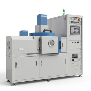
Radio Frequency Plasma Enhanced Chemical Vapor Deposition RF PECVD System for Laboratory and Industrial Thin Film Growth
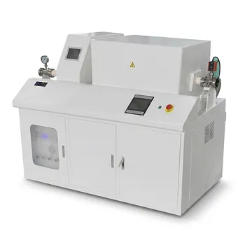
Chemical Vapor Deposition CVD System Slide PECVD Tube Furnace with Liquid Gasifier PECVD Machine
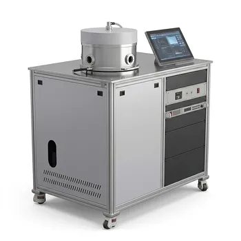
Inclined Rotary Plasma Enhanced Chemical Vapor Deposition PECVD System for Thin Film Deposition and Nanomaterial Synthesis
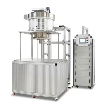
915MHz MPCVD Diamond Machine Microwave Plasma Chemical Vapor Deposition System Reactor
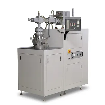
Cylindrical Resonator MPCVD Machine System for Microwave Plasma Chemical Vapor Deposition and Lab Diamond Growth
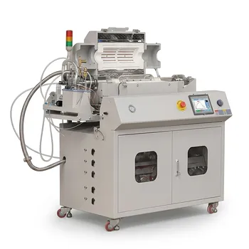
Versatile Chemical Vapor Deposition Tube Furnace System for Advanced Material Research and Industrial Coating Processes
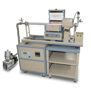
1200C Max Compact Auto-Sliding PECVD Furnace with 2 Inch Tube and Vacuum Pump
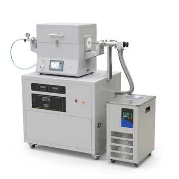
Split Chamber CVD Tube Furnace with Vacuum Station Chemical Vapor Deposition System Machine
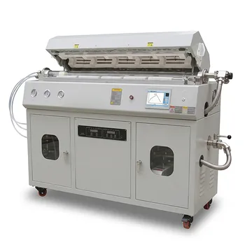
Multi Heating Zones CVD Tube Furnace System for Precision Chemical Vapor Deposition and Advanced Material Synthesis
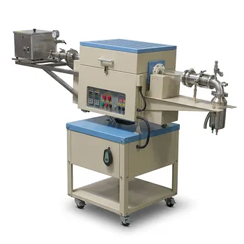
Two Zone Rotary CVD Furnace with Automatic Feeding and Receiving System for Powder Processing
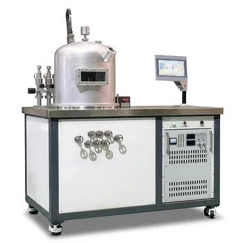
HFCVD Machine System for Nano Diamond Coating on Drawing Dies and Industrial Tools
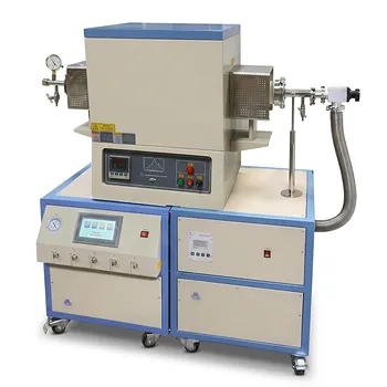
High Temperature 1700C Tube Furnace with High Vacuum Turbomolecular Pump System and Multi Channel Mass Flow Controller Gas Mixer
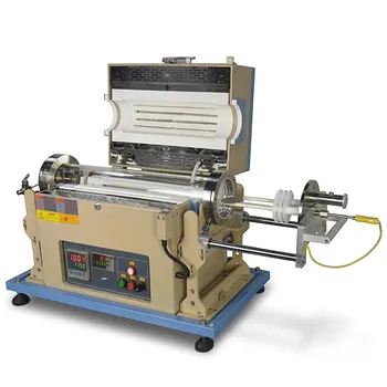
1200°C High Temperature 4 Inch Tube Furnace with Sliding Flange for CVD Systems
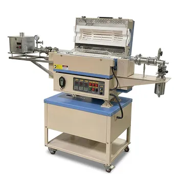
5 Inch Rotary Tube Furnace with Automatic Feeding and Receiving System 1200C Three Zone CVD Powder Processing
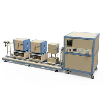
1200C Dual Sliding Tube Furnace with Dual Tubes and Flanges for PECVD Processes
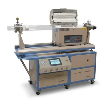
Dual Tube 100mm 80mm CVD Sliding Furnace with 4 Channel Gas Mixing and Vacuum System
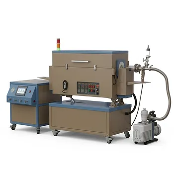
5 Inch Three Zone Rotary Tube Furnace with Integrated Gas Delivery System and 1200C Capability for Advanced Material CVD Processing
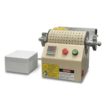
1000C Mini Tube Furnace with 20mm Quartz Tube and Vacuum Flanges for Material Science Research and Controlled Atmosphere Small Sample Processing
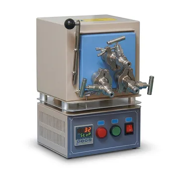
Triple Tube Compact Hybrid Muffle Furnace 1000C High Vacuum Thermal Processing System