What is the necessity of CVD or PECVD for oxide layers on InP? Enhancing Device Performance and Surface Passivation
Updated 3 weeks ago
Depositing an oxide layer via CVD or PECVD on an InP substrate is essential for providing critical insulation and surface passivation. These processes allow for the creation of precise photolithographic windows that define the active area of the device while simultaneously reducing surface state density. This technical approach is the primary driver for minimizing dark current and maximizing the signal-to-noise ratio in high-performance photodetectors.
Core Takeaway: Utilizing CVD/PECVD for oxide deposition on InP is a strategic requirement to stabilize the semiconductor surface and define device geometry. It transforms a raw substrate into a functional electronic platform by enhancing specific detectivity and ensuring electrical isolation.
Enhancing Electrical and Optical Performance
Minimizing Dark Current and Surface States
The primary role of the oxide layer is to passivate the InP surface, which inherently possesses a high density of dangling bonds. By applying a high-quality CVD-deposited oxide, you effectively reduce the surface state density, which prevents unwanted carrier recombination. This reduction is the direct cause of lower dark current, allowing the device to operate with much higher sensitivity.
Improving Signal-to-Noise Ratio (SNR)
A cleaner electrical interface directly translates to better device performance metrics. With the reduction of noise-inducing surface states, the specific detectivity of the photodetector is significantly enhanced. This makes CVD/PECVD indispensable for applications requiring a high signal-to-noise ratio, such as weak-signal infrared detection.
Structural Control and Device Architecture
Precise Definition of Photosensitive Areas
CVD and PECVD allow for the deposition of uniform films that can be patterned using photolithography. By etching "windows" into the oxide layer, engineers can precisely limit the effective photosensitive area of the photodetector. This level of geometric control ensures that the device responds only to light in the designated regions, preventing edge effects and stray signals.
Core Dielectric and Insulation Layers
Beyond passivation, these oxide layers serve as the vital insulation needed to separate conductive elements. In complex structures like Graphene Field-Effect Transistors (GFETs) or field-plate architectures, the oxide acts as a dielectric buffer. It supports metal layers and helps manage high-intensity electric fields, which determines the breakdown voltage and overall reliability of the device.
The Technical Necessity of PECVD
Low-Temperature Processing
InP substrates and associated 2D materials like PtSe2 can be sensitive to extreme thermal budgets. Plasma Enhanced Chemical Vapor Deposition (PECVD) is particularly necessary because it uses low-temperature plasma to excite chemical reactions. This allows for high-quality film growth at temperatures as low as 150°C, protecting the substrate from thermal degradation.
Stoichiometric Precision and Uniformity
PECVD systems provide a controlled environment to manipulate the chemical stoichiometry of the film, such as non-stoichiometric silicon oxide (a-SiOx). This precision ensures that the film is uniform across the entire wafer. Such uniformity is a "hardware guarantee" for consistent photoelectric conversion efficiency and stable electrical performance.
Understanding the Trade-offs
Plasma-Induced Damage
While PECVD allows for low-temperature growth, the high-energy plasma can sometimes cause subsurface damage to the InP crystal lattice. Engineers must carefully balance the plasma power to ensure good adhesion and film density without degrading the carrier mobility of the underlying substrate.
Film Stress and Adhesion
Oxide layers deposited via CVD may harbor intrinsic mechanical stress, which can lead to peeling or cracking on delicate substrates. The choice of precursor gases and deposition rates must be optimized to match the thermal expansion coefficients of the InP. Failure to manage this stress can result in long-term reliability issues or mechanical failure of the device layers.
Selecting the Right Deposition Strategy
How to Apply This to Your Project
Choosing between standard CVD and PECVD depends on your specific thermal constraints and the required film quality.
- If your primary focus is Thermal Sensitivity: Utilize PECVD to maintain substrate integrity through low-temperature plasma excitation.
- If your primary focus is Maximum Dielectric Strength: Opt for High-Quality CVD (such as LPCVD) if the substrate can withstand higher temperatures, as it often produces denser, more robust films.
- If your primary focus is Patterning Precision: Ensure the oxide thickness is optimized for photolithographic contrast to define clear windows for the active device area.
The integration of a CVD-deposited oxide layer is the foundational step in transitioning from a bare InP substrate to a high-performance, passivated electronic device.
Summary Table:
| Feature | Benefit to InP Substrate | Technical Advantage |
|---|---|---|
| Surface Passivation | Reduces dark current & surface states | Enhances signal-to-noise ratio (SNR) |
| Electrical Insulation | Vital dielectric for metal separation | High breakdown voltage & reliability |
| Structural Control | Defines active photolithographic areas | Precise geometry for photodetectors |
| Low-Temp Growth | Protects thermal-sensitive materials | PECVD allows films at low temperatures (<150°C) |
Elevate your semiconductor research with high-precision thermal solutions from THERMUNITS. As a leading manufacturer of high-temperature laboratory equipment for material science, we provide advanced CVD and PECVD systems designed for critical processes like oxide deposition on InP substrates. Our equipment ensures uniform film growth and precise stoichiometric control to maximize your device's signal-to-noise ratio and electrical stability.
Beyond vapor deposition, THERMUNITS offers a comprehensive range of thermal processing solutions, including Muffle, Vacuum, Atmosphere, Tube, and Rotary furnaces, as well as Dental Furnaces, Vacuum Induction Melting (VIM) systems, and high-quality Thermal Elements.
Ready to optimize your R&D workflow? Contact our technical experts today for a customized quote!
References
- Jiang Wang, Lin‐Bao Luo. PtSe<sub>2</sub>/InP Mixed‐Dimensional Schottky Junction for High‐Performance Self‐Powered Near‐Infrared Photodetection. DOI: 10.1002/adom.202401035
Mentioned Products
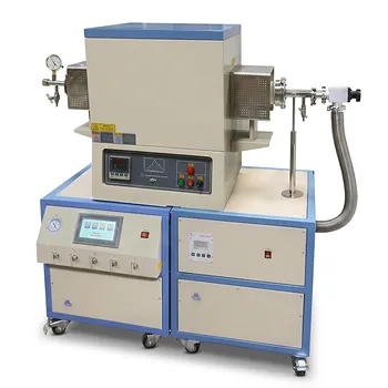
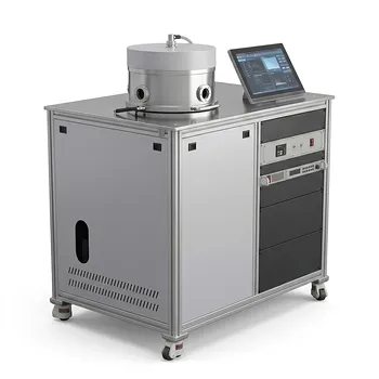
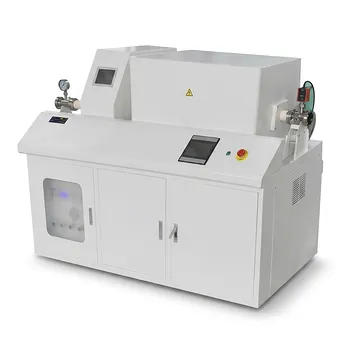
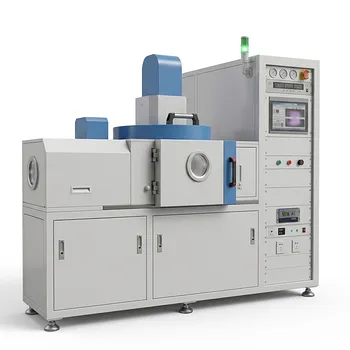
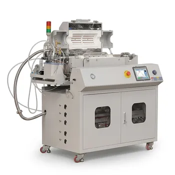
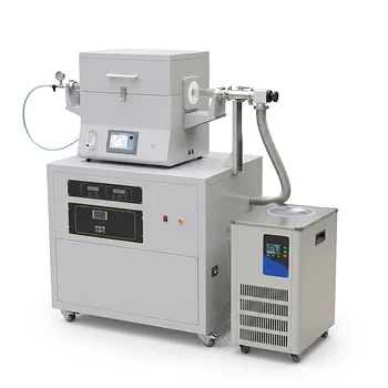
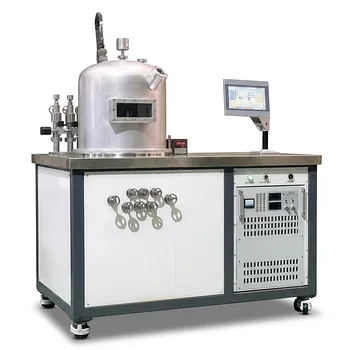
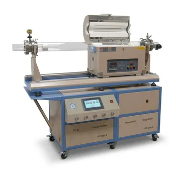
- Inclined Rotary Plasma Enhanced Chemical Vapor Deposition PECVD System for Thin Film Deposition and Nanomaterial Synthesis
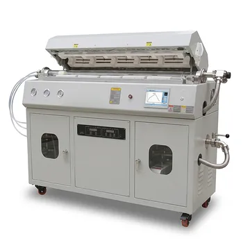
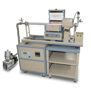
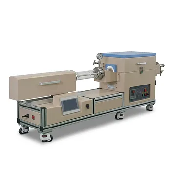
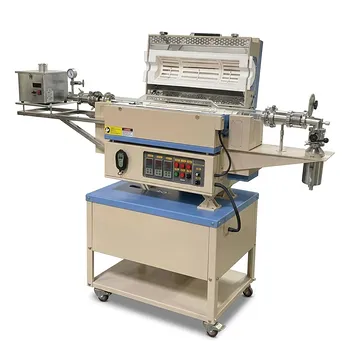
- Chemical Vapor Deposition CVD System Slide PECVD Tube Furnace with Liquid Gasifier PECVD Machine
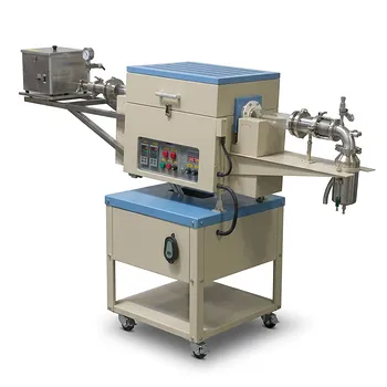
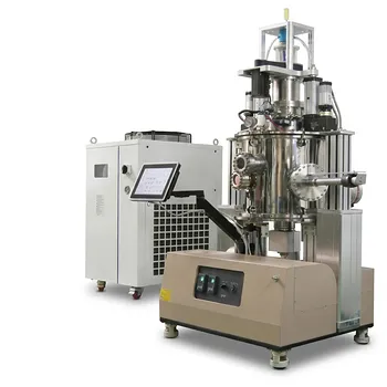
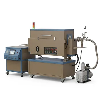
- Radio Frequency Plasma Enhanced Chemical Vapor Deposition RF PECVD System for Laboratory and Industrial Thin Film Growth
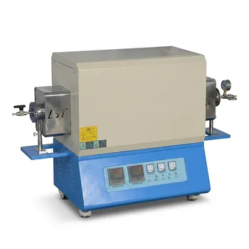
- Versatile Chemical Vapor Deposition Tube Furnace System for Advanced Material Research and Industrial Coating Processes
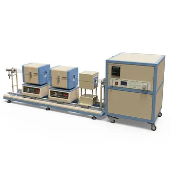
- Multi Heating Zones CVD Tube Furnace System for Precision Chemical Vapor Deposition and Advanced Material Synthesis
People Also Ask
- Why is it necessary to strictly control the flow of argon gas during the preparation of f-SWNTs-T catalysts? | Optimize R&D
- Why is CVD preferred over PVD for high-aspect-ratio features? Superior Conformality for Semiconductor Fabrication
- What are the primary technical variants and capabilities of CVD systems? Master High-Purity Material Synthesis
- How do Chemical Vapor Deposition (CVD) coatings enhance industrial tools? Boost Tool Life and Wear Resistance
- What is the role of CVD/PECVD systems in the research of optoelectronic materials and functional coatings? Expert Guide
Tech Team · ThermUnits
Last updated on Jun 02, 2026
Related Products
Inclined Rotary Plasma Enhanced Chemical Vapor Deposition PECVD System for Thin Film Deposition and Nanomaterial Synthesis
Chemical Vapor Deposition CVD System Slide PECVD Tube Furnace with Liquid Gasifier PECVD Machine
Radio Frequency Plasma Enhanced Chemical Vapor Deposition RF PECVD System for Laboratory and Industrial Thin Film Growth
Versatile Chemical Vapor Deposition Tube Furnace System for Advanced Material Research and Industrial Coating Processes
Multi Heating Zones CVD Tube Furnace System for Precision Chemical Vapor Deposition and Advanced Material Synthesis
915MHz MPCVD Diamond Machine Microwave Plasma Chemical Vapor Deposition System Reactor
Cylindrical Resonator MPCVD Machine System for Microwave Plasma Chemical Vapor Deposition and Lab Diamond Growth
Split Chamber CVD Tube Furnace with Vacuum Station Chemical Vapor Deposition System Machine
1200C Max Compact Auto-Sliding PECVD Furnace with 2 Inch Tube and Vacuum Pump
1200C Dual Sliding Tube Furnace with Dual Tubes and Flanges for PECVD Processes
Two Zone Rotary CVD Furnace with Automatic Feeding and Receiving System for Powder Processing
HFCVD Machine System for Nano Diamond Coating on Drawing Dies and Industrial Tools
1200C Sliding Internal Crucible Tube Furnace for Controlled Atmosphere Thin Film Deposition and Material Sublimation Research
High Temperature Dual Zone Vacuum Tube Furnace for Material Research and CVD Processing
950C Rapid Thermal Processing Furnace for 12 Inch Wafer CSS Coating with Rotating Substrate Holder
Dual Tube 100mm 80mm CVD Sliding Furnace with 4 Channel Gas Mixing and Vacuum System
High Pressure Induction Melting Casting System 1700C Max for Alloy Granulation and Infiltration Equipment
5 Inch Rotary Tube Furnace with Automatic Feeding and Receiving System 1200C Three Zone CVD Powder Processing
5 Inch Three Zone Rotary Tube Furnace with Integrated Gas Delivery System and 1200C Capability for Advanced Material CVD Processing