What is the purpose of using a PECVD system for doping polycrystalline silicon? Improve carrier control & conductivity.
Updated 6 days ago
In the fabrication of polycrystalline silicon layers, the primary purpose of a Plasma-Enhanced Chemical Vapor Deposition (PECVD) system is to deposit a thin, phosphorus-doped amorphous silicon (a-Si:P) layer. This layer serves as a high-precision doping source, providing the phosphorus atoms that will eventually diffuse into the polycrystalline silicon during subsequent thermal processing to define its electrical characteristics.
Core Takeaway: PECVD is used to create a sacrificial or precursor "doping reservoir" on the silicon surface. By depositing a uniform amorphous layer at low temperatures, manufacturers can achieve precise control over carrier concentration and conductivity while avoiding the physical and chemical drawbacks of traditional high-temperature diffusion methods.
The Role of PECVD as a Doping Source
Creating the Amorphous Reservoir
The PECVD system utilizes plasma-assisted decomposition of precursor gases, typically silane (SiH4) and phosphine (PH3), to form the a-Si:P layer. This layer is not the final contact but acts as a concentrated source of dopant atoms.
Facilitating Thermal Diffusion
Once the amorphous layer is deposited, a subsequent high-temperature annealing process is required. During this step, phosphorus atoms migrate from the a-Si:P layer into the underlying polycrystalline silicon, precisely setting the carrier concentration and conductivity type.
Precise Concentration Control
By adjusting the flow ratio of precursor gases within the PECVD chamber, engineers can achieve a highly uniform doping distribution. This level of control is essential for the performance of modern semiconductor devices and high-efficiency solar cells.
Technical Advantages Over Conventional Methods
Lower Thermal Stress
Unlike Low-Pressure Chemical Vapor Deposition (LPCVD) or traditional diffusion, PECVD operates at significantly lower substrate temperatures. This protects temperature-sensitive materials and prevents the physical warping or damage to quartz furnace tubes often seen in high-heat processes.
Single-Sided Deposition and Precision
One of the most critical industrial advantages of PECVD is its support for single-sided deposition. This effectively eliminates the "wrap-around effect" common in diffusion furnaces, where dopants unintentionally coat the edges or rear of the wafer.
High Precursor Utilization
PECVD systems offer high silane (SiH4) utilization rates, making the process more cost-effective for large-scale industrial production. The highly reactive radicals generated by the plasma allow for rapid film growth without requiring excessive gas consumption.
Understanding the Trade-offs
The Requirement for Post-Processing
While PECVD is excellent for deposition, the deposited layer is amorphous and the dopants are not yet "active." A secondary thermal treatment is mandatory to crystallize the layer and drive the dopants into the silicon lattice.
Plasma Damage Risks
The use of high-energy ions and radicals can occasionally lead to surface damage or unintended charge trapping. This necessitates careful calibration of the RF or microwave power to balance deposition speed with film quality.
Stoichiometry Complexity
Maintaining the exact chemical stoichiometry of the thin film requires sophisticated control systems. Small fluctuations in gas pressure or plasma power can alter the refractive index or dopant density, potentially impacting the final device's optical or electrical performance.
Applying PECVD to Your Production Goals
Recommendations for Implementation
The decision to use PECVD for doping depends on your specific device architecture and thermal budget requirements.
- If your primary focus is high-efficiency solar cells: Use PECVD to deposit a-Si:P layers that allow for hydrogen-induced passivation and precise anti-reflection coating control.
- If your primary focus is minimizing manufacturing defects: Leverage PECVD’s single-sided deposition capability to avoid the wrap-around effect and reduce the need for subsequent edge-isolation steps.
- If your primary focus is processing temperature-sensitive substrates: Prioritize PECVD over LPCVD to maintain a lower thermal budget and prevent structural damage to the wafer or carrier.
By utilizing PECVD as a controlled doping source, you bridge the gap between low-temperature film deposition and high-performance electrical conductivity.
Summary Table:
| Feature | Advantage of PECVD in Doping | Impact on Fabrication |
|---|---|---|
| Deposition Type | Single-sided deposition | Eliminates "wrap-around" effects on wafers |
| Temperature | Low-temperature processing | Reduces thermal stress and substrate damage |
| Dopant Source | Phosphorus-doped amorphous silicon (a-Si:P) | Provides a high-precision reservoir for diffusion |
| Efficiency | High silane (SiH4) utilization | Lowers production costs and gas consumption |
| Control | Precise gas flow ratios | Achieves uniform carrier concentration |
Elevate Your Material Research with THERMUNITS
Optimize your semiconductor and solar cell fabrication with precision thermal solutions from THERMUNITS. As a leading manufacturer of high-temperature laboratory equipment, we specialize in providing advanced CVD/PECVD systems, Tube furnaces, and Atmosphere furnaces tailored for high-performance R&D and industrial applications.
Whether you require Muffle, Vacuum, or Rotary kilns, or specialized Vacuum Induction Melting (VIM) systems, our equipment is designed to ensure maximum uniformity and process control.
Ready to enhance your lab’s capabilities? Contact our technical experts today to find the perfect heat treatment solution for your specific material science needs.
References
- David L. Young, Melbs LeMieux. Metal-Complex Inks for Lower Cost and Improved Passivation for Silicon Photovoltaic Metallization. DOI: 10.52825/siliconpv.v1i.853
Mentioned Products
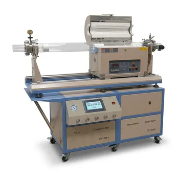
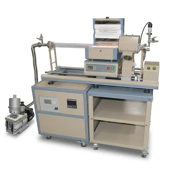
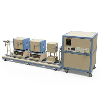
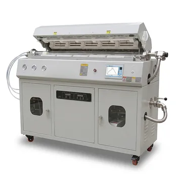
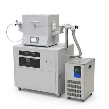
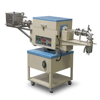
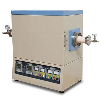
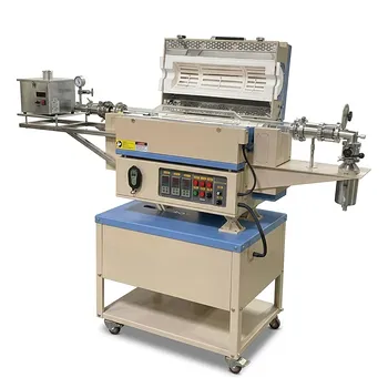
- Chemical Vapor Deposition CVD System Slide PECVD Tube Furnace with Liquid Gasifier PECVD Machine
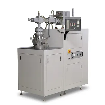
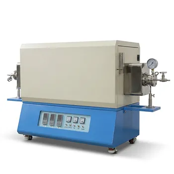
- Inclined Rotary Plasma Enhanced Chemical Vapor Deposition PECVD System for Thin Film Deposition and Nanomaterial Synthesis
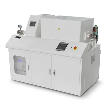
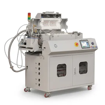
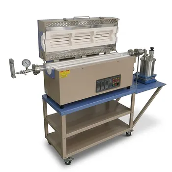
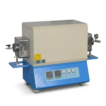
- Radio Frequency Plasma Enhanced Chemical Vapor Deposition RF PECVD System for Laboratory and Industrial Thin Film Growth
- 1200C Max Compact Auto-Sliding PECVD Furnace with 2 Inch Tube and Vacuum Pump
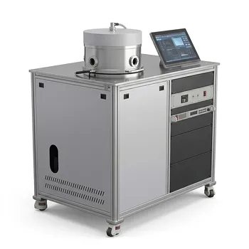
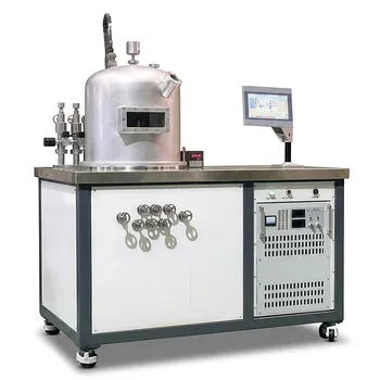
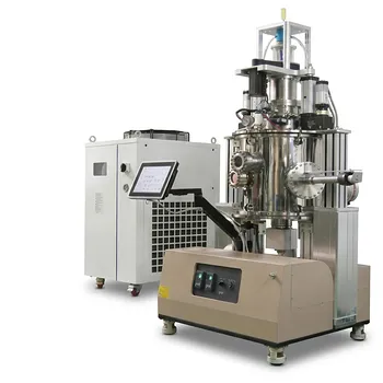
- Cylindrical Resonator MPCVD Machine System for Microwave Plasma Chemical Vapor Deposition and Lab Diamond Growth
People Also Ask
- What are the technical advantages of the electrodeless plasma design in MPCVD systems? Purity & Precision in Synthesis
- Why is it necessary to strictly control the flow of argon gas during the preparation of f-SWNTs-T catalysts? | Optimize R&D
- In what ways does Chemical Vapor Deposition (CVD) improve solar cells? Enhance Efficiency with Precise Thin-Film Coating
- How do Chemical Vapor Deposition (CVD) coatings enhance industrial tools? Boost Tool Life and Wear Resistance
- How does the use of helium gas flow control affect the DM process? Enhance Precision in CVD Graphene Synthesis
Tech Team · ThermUnits
Last updated on Jun 02, 2026
Related Products
Chemical Vapor Deposition CVD System Slide PECVD Tube Furnace with Liquid Gasifier PECVD Machine
Inclined Rotary Plasma Enhanced Chemical Vapor Deposition PECVD System for Thin Film Deposition and Nanomaterial Synthesis
Radio Frequency Plasma Enhanced Chemical Vapor Deposition RF PECVD System for Laboratory and Industrial Thin Film Growth
1200C Max Compact Auto-Sliding PECVD Furnace with 2 Inch Tube and Vacuum Pump
Cylindrical Resonator MPCVD Machine System for Microwave Plasma Chemical Vapor Deposition and Lab Diamond Growth
915MHz MPCVD Diamond Machine Microwave Plasma Chemical Vapor Deposition System Reactor
Versatile Chemical Vapor Deposition Tube Furnace System for Advanced Material Research and Industrial Coating Processes
1200C Dual Sliding Tube Furnace with Dual Tubes and Flanges for PECVD Processes
Multi Heating Zones CVD Tube Furnace System for Precision Chemical Vapor Deposition and Advanced Material Synthesis
Split Chamber CVD Tube Furnace with Vacuum Station Chemical Vapor Deposition System Machine
Two Zone Rotary CVD Furnace with Automatic Feeding and Receiving System for Powder Processing
High Temperature 1700C Dual Zone Tube Furnace for Material Science and Industrial Chemical Vapor Deposition Research
HFCVD Machine System for Nano Diamond Coating on Drawing Dies and Industrial Tools
Three Temperature Zone High Temperature Vacuum Tube Furnace for CVD and Material Sintering
5 Inch Two Zone Rotary Tube Furnace 1100C for Powder CVD and Material Synthesis
5 Inch Rotary Tube Furnace with Automatic Feeding and Receiving System 1200C Three Zone CVD Powder Processing
High Temperature Dual Zone Vacuum Tube Furnace for Material Research and CVD Processing
1000C Mini Tube Furnace with 20mm Quartz Tube and Vacuum Flanges for Material Science Research and Controlled Atmosphere Small Sample Processing
950C Rapid Thermal Processing Furnace for 12 Inch Wafer CSS Coating with Rotating Substrate Holder