What role does hydrogen play in PECVD films for solar? Enhancing Passivation and Efficiency
Updated 5 months ago
Hydrogen acts as the primary chemical agent for defect neutralization and surface optimization in PECVD-deposited films. By diffusing from hydrogen-rich layers—such as silicon nitride ($SiN_x$) or amorphous silicon ($a\text{-}Si$)—into the silicon substrate, hydrogen "heals" atomic-level defects. This process is the foundation for achieving high open-circuit voltages and superior fill factors, allowing modern solar modules to reach conversion efficiencies exceeding 25%.
Core Takeaway: Hydrogen is not merely a byproduct of the PECVD process; it is a functional tool used to passivate recombination centers and chemically clean the wafer surface, making high-efficiency solar cell architectures like TOPCon and HJT commercially viable.
The Mechanics of Defect Passivation
Neutralizing Surface Dangling Bonds
At the interface between the silicon wafer and the deposited film, "dangling bonds" act as traps for charge carriers. Hydrogen atoms chemically bond with these unsatisfied silicon bonds, effectively removing the energy states that cause carrier recombination. This surface passivation ensures that electrons and holes can be collected efficiently rather than being lost at the boundary.
Bulk Passivation through Diffusion
During the PECVD process, hydrogen does not stay confined to the deposited film. It diffuses deep into the bulk of the silicon wafer, where it interacts with impurities and structural defects. This internal "healing" significantly improves the minority carrier lifetime throughout the entire thickness of the cell.
Impact on Electrical Performance
The primary result of effective passivation is a dramatic increase in Open-Circuit Voltage ($V_{oc}$) and Fill Factor (FF). By reducing the number of sites where energy is lost, hydrogen allows the solar cell to maintain a higher voltage under load, which is critical for pushing efficiency boundaries in PERC and TOPCon designs.
Hydrogen as a Chemical Cleaning Agent
Removal of Organic Contaminants
Hydrogen plasma treatment is often employed within the PECVD system to prepare the substrate. High-energy hydrogen ions react with residual organic impurities, converting them into volatile gases that are pumped out of the chamber. This creates an atomically clean surface, which is a prerequisite for the uniform growth of high-quality thin films.
Reduction of Native Oxides
Before the growth of films like Hexagonal Boron Nitride or specialized silicon layers, hydrogen acts as a reducing agent. It helps remove unwanted oxide layers from the metal or silicon surface. This "surface planarization" ensures that the subsequent epitaxial growth is defect-free and structurally sound.
Etching of Amorphous Byproducts
In advanced thin-film growth, hydrogen can act as a selective etching agent. It removes non-crystalline or "amorphous" carbon and silicon species that might otherwise clog the reaction site or poison the catalysts. This selective etching maintains the purity and crystallinity of the functional solar layers.
Understanding the Trade-offs and Challenges
Thermal Stability and Effusion
While hydrogen is beneficial, its bond with silicon is sensitive to high temperatures. If a solar cell is subjected to excessive heat during subsequent manufacturing steps, hydrogen can "effuse" or escape the film. This loss of hydrogen leads to a sudden drop in passivation quality and overall cell efficiency.
Light-Induced Degradation (LID)
In some hydrogen-rich films, particularly amorphous silicon, the presence of hydrogen is linked to the Staebler-Wronski effect. Under prolonged sunlight exposure, the metastable nature of the Si-H bonds can cause a slight decrease in efficiency over time. Engineers must carefully balance the hydrogen concentration to maximize initial passivation while ensuring long-term stability.
Stoichiometry Control
Excessive hydrogen can alter the refractive index and chemical stoichiometry of anti-reflective coatings like $SiN_x$. If the hydrogen content is not precisely controlled via the silane-to-ammonia ratio, the film may become too absorbing or fail to provide the necessary optical properties for maximum photon capture.
How to Optimize Hydrogen Utilization
Application Strategies for Solar Projects
- If your primary focus is Surface Passivation (HJT Cells): Prioritize intrinsic amorphous silicon layers ($a\text{-}Si:H$) with high hydrogen content to minimize interface recombination.
- If your primary focus is Anti-Reflective Coatings (PERC/TOPCon): Use hydrogen-rich silicon nitride ($SiN_x:H$) to provide a dual benefit of light management and bulk defect healing during the firing process.
- If your primary focus is Substrate Preparation: Implement a hydrogen plasma pre-treatment step to volatilize organics and ensure the highest possible adhesion for subsequent thin films.
When managed with precision, hydrogen is the "secret ingredient" that transforms a standard silicon wafer into a high-performance semiconductor device.
Summary Table:
| Role of Hydrogen | Mechanism of Action | Impact on Solar Performance |
|---|---|---|
| Surface Passivation | Neutralizes "dangling bonds" at the Si interface | Increases Open-Circuit Voltage (Voc) and Fill Factor |
| Bulk Passivation | Diffuses into substrate to heal internal defects | Significantly improves minority carrier lifetime |
| Chemical Cleaning | Removes organic contaminants via plasma reaction | Ensures atomic cleanliness and uniform film growth |
| Oxide Reduction | Acts as a reducing agent for native oxides | Facilitates defect-free epitaxial growth |
| Selective Etching | Removes amorphous carbon or silicon species | Maintains high purity and crystallinity of layers |
Maximize Your Solar R&D Precision with THERMUNITS
To achieve industry-leading conversion efficiencies, your thermal processing must be flawless. THERMUNITS is a leading manufacturer of high-temperature laboratory equipment specifically designed for material science and industrial R&D.
We offer a comprehensive range of high-performance solutions, including:
- Advanced CVD/PECVD Systems for precise film deposition.
- Specialized Furnaces: Muffle, Vacuum, Atmosphere, Tube, Rotary, and Hot Press furnaces.
- Industrial Equipment: Electric rotary kilns, Vacuum Induction Melting (VIM) furnaces, and Dental Furnaces.
- Thermal Elements and customized heat treatment components.
Whether you are optimizing hydrogen passivation for TOPCon cells or developing next-generation semiconductors, our equipment delivers the control and reliability you need.
Contact THERMUNITS today to discuss your project requirements!
Mentioned Products
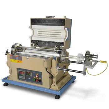
- Chemical Vapor Deposition CVD System Slide PECVD Tube Furnace with Liquid Gasifier PECVD Machine
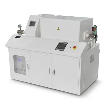
- Inclined Rotary Plasma Enhanced Chemical Vapor Deposition PECVD System for Thin Film Deposition and Nanomaterial Synthesis
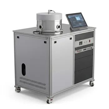
- Radio Frequency Plasma Enhanced Chemical Vapor Deposition RF PECVD System for Laboratory and Industrial Thin Film Growth
- 1200C Max Compact Auto-Sliding PECVD Furnace with 2 Inch Tube and Vacuum Pump
- 1200C Dual Sliding Tube Furnace with Dual Tubes and Flanges for PECVD Processes
People Also Ask
- What are the advantages of PECVD systems for nano flame retardant films? Protect Heat-Sensitive Polymers with Precision
- How does a sliding rail design benefit the CVD process within a furnace ventilation hood? Enhance Control & Quenching
- What is the role of CVD/PECVD systems in the research of optoelectronic materials and functional coatings? Expert Guide
- How does PECVD differ from conventional thermal CVD? Key Advantages of Low-Temperature Deposition for R&D
- What role do by-product desorption and evacuation play in CVD film quality? Key Factors for High-Purity Films

Tech Team · ThermUnits
Last updated on Apr 14, 2026
Related Products
Chemical Vapor Deposition CVD System Slide PECVD Tube Furnace with Liquid Gasifier PECVD Machine
Inclined Rotary Plasma Enhanced Chemical Vapor Deposition PECVD System for Thin Film Deposition and Nanomaterial Synthesis
Radio Frequency Plasma Enhanced Chemical Vapor Deposition RF PECVD System for Laboratory and Industrial Thin Film Growth
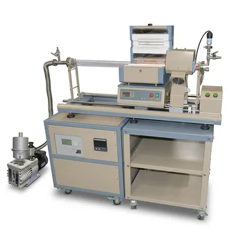
1200C Max Compact Auto-Sliding PECVD Furnace with 2 Inch Tube and Vacuum Pump
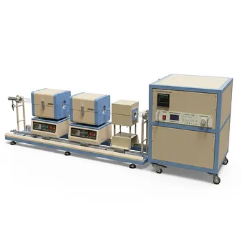
1200C Dual Sliding Tube Furnace with Dual Tubes and Flanges for PECVD Processes
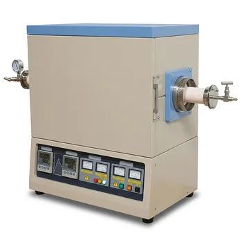
High Temperature 1700C Dual Zone Tube Furnace for Material Science and Industrial Chemical Vapor Deposition Research
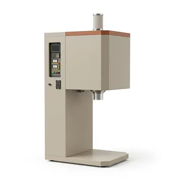
Vertical Openable Tube Furnace 0-1700c High Temperature Laboratory System for CVD and Vacuum Heat Treatment
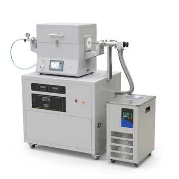
Split Chamber CVD Tube Furnace with Vacuum Station Chemical Vapor Deposition System Machine
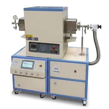
High Temperature 1700C Tube Furnace with High Vacuum Turbomolecular Pump System and Multi Channel Mass Flow Controller Gas Mixer
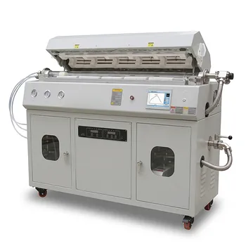
Multi Heating Zones CVD Tube Furnace System for Precision Chemical Vapor Deposition and Advanced Material Synthesis
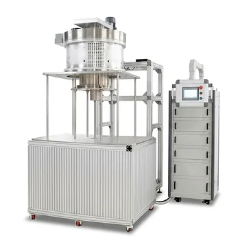
915MHz MPCVD Diamond Machine Microwave Plasma Chemical Vapor Deposition System Reactor
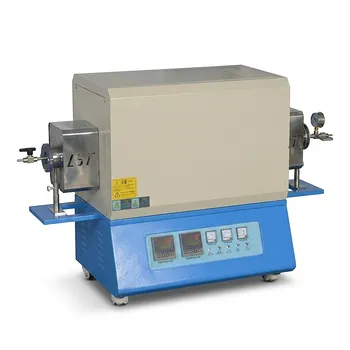
High Temperature Dual Zone Vacuum Tube Furnace for Material Research and CVD Processing
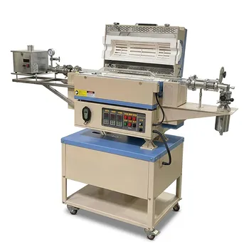
5 Inch Rotary Tube Furnace with Automatic Feeding and Receiving System 1200C Three Zone CVD Powder Processing
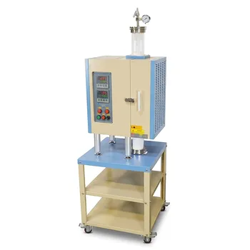
1100°C Dual Zone Split Vertical Tube Furnace with 4 Inch Quartz Tube and Vacuum Sealing Flanges
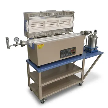
5 Inch Two Zone Rotary Tube Furnace 1100C for Powder CVD and Material Synthesis
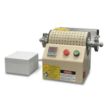
1000C Mini Tube Furnace with 20mm Quartz Tube and Vacuum Flanges for Material Science Research and Controlled Atmosphere Small Sample Processing
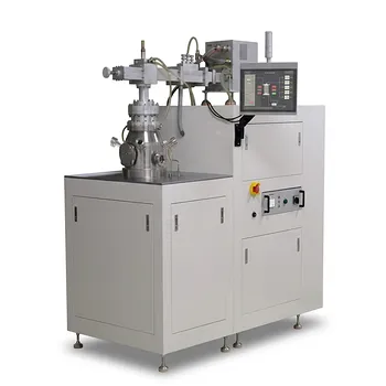
Cylindrical Resonator MPCVD Machine System for Microwave Plasma Chemical Vapor Deposition and Lab Diamond Growth
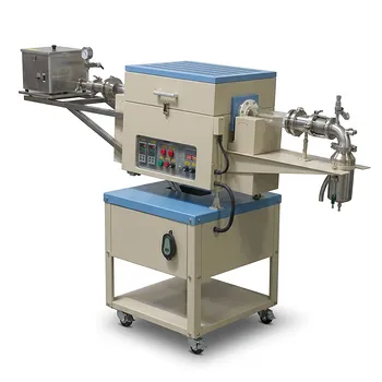
Two Zone Rotary CVD Furnace with Automatic Feeding and Receiving System for Powder Processing
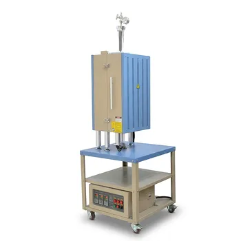
1200C Three Zone Vertical Tube Furnace with 2 Inch Quartz Tube and Vacuum Flanges