Why is a Low-Pressure Chemical Vapor Deposition (LPCVD) system necessary? High-Efficiency TOPCon Solar Cell Solutions
Updated 1 month ago
LPCVD systems are essential because they provide the precise structural density and uniform step coverage required for high-efficiency carrier-selective contacts. This technology enables the deposition of a dense, 200 nm polycrystalline silicon (poly-Si) layer that ensures efficient carrier transport while maintaining the integrity of the underlying tunnel oxide.
LPCVD is the industry standard for TOPCon solar cells because it creates a high-purity, dense film with exceptional thickness uniformity. This structural consistency is the foundation for effective surface passivation and reliable electrical performance across the entire silicon wafer.
Superior Film Quality and Structural Integrity
Excellent Step Coverage on Textured Surfaces
Solar cell surfaces are often textured to maximize light absorption, creating a complex topography that is difficult to coat. LPCVD operates at low pressures, which increases the mean free path of gas molecules and allows them to deposit uniformly into every micro-texture. This ensures the poly-Si layer maintains a consistent thickness, preventing "thin spots" that could lead to electrical shunting.
Dense Film Structure for Carrier Transport
The primary reference highlights that LPCVD produces a highly dense film structure compared to other deposition methods. This density is critical for constructing high-quality passivation contact interfaces that facilitate efficient carrier movement. A porous film would degrade the cell’s internal electronics and reduce the overall conversion efficiency.
High Purity and Uniform Grain Structure
Using high-purity silane gas at controlled temperatures (typically around 530°C) results in a film with a uniform grain structure. This uniformity ensures a consistent work function across the wafer, which is vital for maintaining a reliable electric field distribution. Without this consistency, individual cells in a production batch would vary significantly in performance.
Enhancing Electrical Performance in TOPCon Cells
Synergistic Passivation with Tunnel Oxide
In TOPCon (Tunnel Oxide Passivated Contact) architectures, the LPCVD system is used to deposit the poly-Si layer directly over an ultra-thin tunnel oxide. The precision of LPCVD ensures that the poly-Si layer acts as an effective carrier-selective contact. This allows for carrier tunneling while simultaneously providing the chemical passivation needed to reduce surface recombination.
Precise Control Over Doping Diffusion
LPCVD films provide a stable foundation for in-situ doping or subsequent diffusion steps. Because the film thickness is so uniform, phosphorus or other dopants can migrate through the poly-Si layer at a predictable rate. This results in consistent carrier concentration and conductivity types, which are necessary for high-efficiency mass production.
Mechanical Stability and Stress Management
The high-precision nature of LPCVD allows manufacturers to adjust gas flow rates to manage internal tensile stress. Maintaining low residual stress (often around 100 MPa) prevents the thin films from cracking or delaminating during subsequent high-temperature manufacturing steps. This mechanical durability is essential for the long-term reliability of the solar module.
Understanding the Trade-offs
Thermal Budget and Process Speed
While LPCVD offers superior film quality, it requires medium to high temperatures (500°C to 600°C), which adds to the thermal budget of the manufacturing process. This is significantly higher than Plasma-Enhanced Chemical Vapor Deposition (PECVD), which can operate at lower temperatures but may not achieve the same level of film density.
Maintenance and Wrap-around Effects
LPCVD systems often face challenges with "wrap-around" deposition, where the silicon film deposits on the edges or back of the wafer. This necessitates additional cleaning or etching steps in the production line. However, the trade-off is generally considered acceptable given the significant boost in cell efficiency provided by the high-quality LPCVD film.
How to Apply This to Your Solar Project
Choosing the Right Deposition Strategy
- If your primary focus is maximum conversion efficiency (e.g., TOPCon cells): LPCVD is the necessary choice to ensure the density and step coverage required for high-quality passivation contacts.
- If your primary focus is high throughput and low thermal budget: Consider PECVD for non-critical layers like anti-reflective coatings, but recognize it may not provide the same contact quality as LPCVD for poly-Si layers.
- If your primary focus is consistent mass production: Prioritize LPCVD for its ability to provide uniform grain structures and predictable doping diffusion across large batches of wafers.
LPCVD remains the definitive technology for high-performance solar contacts because it balances structural density with the extreme precision required for modern photovoltaic architectures.
Summary Table:
| Feature | Advantage of LPCVD | Impact on Solar Cell Performance |
|---|---|---|
| Step Coverage | Excellent on textured surfaces | Prevents electrical shunting and thin spots |
| Film Density | Highly dense polycrystalline silicon | Facilitates efficient carrier transport |
| Purity | Uniform grain structure (Silane gas) | Ensures consistent work function across wafer |
| Stress Control | Low residual tensile stress (~100 MPa) | Prevents cracking during high-temp processing |
| Doping Control | Stable base for diffusion/in-situ doping | Predictable conductivity and carrier concentration |
Optimize Your Research with THERMUNITS Thermal Solutions
Enhance your material science and industrial R&D with THERMUNITS, a leading manufacturer of high-temperature laboratory equipment. We provide a comprehensive range of thermal processing solutions designed for precision and reliability, including:
- CVD/PECVD Systems & LPCVD-compatible setups
- Furnaces: Muffle, Vacuum, Atmosphere, Tube, Rotary, and Hot Press furnaces
- Specialized Equipment: Dental Furnaces, Electric Rotary Kilns, and Vacuum Induction Melting Furnaces (VIM)
- Thermal Elements and various laboratory heat treatment tools
Whether you are developing next-generation TOPCon solar cells or conducting advanced metallurgical studies, our equipment delivers the uniform heating and atmospheric control you need.
Ready to elevate your lab's performance? Contact us today to discuss your project requirements!
References
- David L. Young, Melbs LeMieux. Metal-Complex Inks for Lower Cost and Improved Passivation for Silicon Photovoltaic Metallization. DOI: 10.52825/siliconpv.v1i.853
Mentioned Products
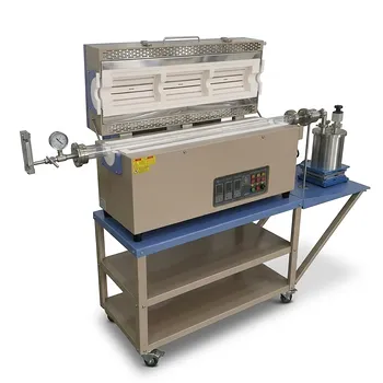
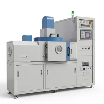
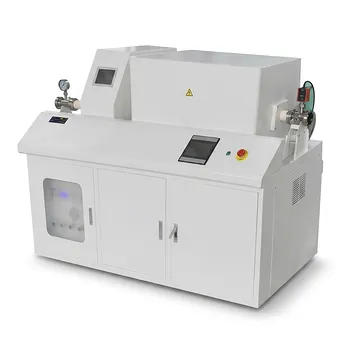
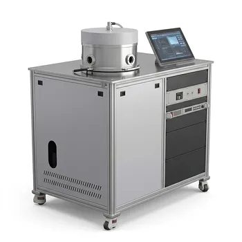
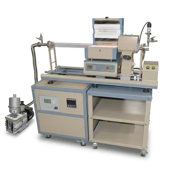
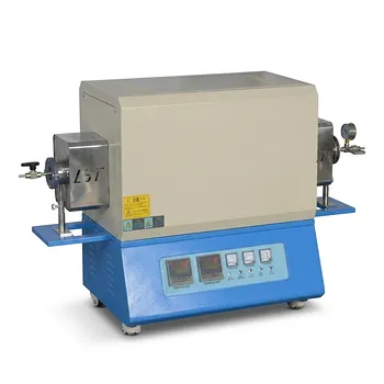
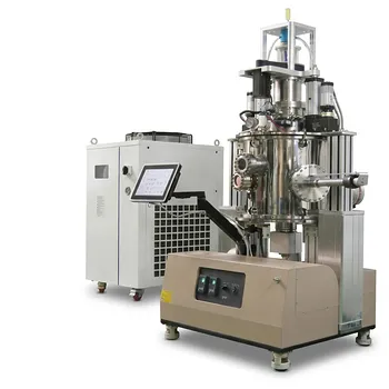
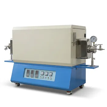
- Radio Frequency Plasma Enhanced Chemical Vapor Deposition RF PECVD System for Laboratory and Industrial Thin Film Growth
- Chemical Vapor Deposition CVD System Slide PECVD Tube Furnace with Liquid Gasifier PECVD Machine
- Inclined Rotary Plasma Enhanced Chemical Vapor Deposition PECVD System for Thin Film Deposition and Nanomaterial Synthesis
- Versatile Chemical Vapor Deposition Tube Furnace System for Advanced Material Research and Industrial Coating Processes
- Cylindrical Resonator MPCVD Machine System for Microwave Plasma Chemical Vapor Deposition and Lab Diamond Growth
People Also Ask
- How does a Chemical Vapor Deposition (CVD) system ensure product quality? Precision Control for 2D Nanomaterial Growth
- How does the non-equilibrium nature of plasma facilitate low-temperature deposition in PECVD systems? Pro Tips for R&D
- How do RF frequency and power settings influence the characteristics of a PECVD process? Master Quality & Efficiency
- How is Plasma-Enhanced Chemical Vapor Deposition (PECVD) utilized in the production of photovoltaic solar cells? Study
- How do temperature regimes influence the growth rate of films in a CVD system? Master CVD Kinetics for Superior Thin Films
Tech Team · ThermUnits
Last updated on Jun 02, 2026
Related Products
Radio Frequency Plasma Enhanced Chemical Vapor Deposition RF PECVD System for Laboratory and Industrial Thin Film Growth
Chemical Vapor Deposition CVD System Slide PECVD Tube Furnace with Liquid Gasifier PECVD Machine
Inclined Rotary Plasma Enhanced Chemical Vapor Deposition PECVD System for Thin Film Deposition and Nanomaterial Synthesis
Versatile Chemical Vapor Deposition Tube Furnace System for Advanced Material Research and Industrial Coating Processes
Cylindrical Resonator MPCVD Machine System for Microwave Plasma Chemical Vapor Deposition and Lab Diamond Growth
915MHz MPCVD Diamond Machine Microwave Plasma Chemical Vapor Deposition System Reactor
Multi Heating Zones CVD Tube Furnace System for Precision Chemical Vapor Deposition and Advanced Material Synthesis
Split Chamber CVD Tube Furnace with Vacuum Station Chemical Vapor Deposition System Machine
Two Zone Rotary CVD Furnace with Automatic Feeding and Receiving System for Powder Processing
HFCVD Machine System for Nano Diamond Coating on Drawing Dies and Industrial Tools
1200C Sliding Internal Crucible Tube Furnace for Controlled Atmosphere Thin Film Deposition and Material Sublimation Research
1200C Max Compact Auto-Sliding PECVD Furnace with 2 Inch Tube and Vacuum Pump
High Temperature Dual Zone Vacuum Tube Furnace for Material Research and CVD Processing
950C Rapid Thermal Processing Furnace for 12 Inch Wafer CSS Coating with Rotating Substrate Holder
Three Temperature Zone High Temperature Vacuum Tube Furnace for CVD and Material Sintering
1000C Mini Tube Furnace with 20mm Quartz Tube and Vacuum Flanges for Material Science Research and Controlled Atmosphere Small Sample Processing
5 Inch Three Zone Rotary Tube Furnace with Integrated Gas Delivery System and 1200C Capability for Advanced Material CVD Processing
Dual Tube 100mm 80mm CVD Sliding Furnace with 4 Channel Gas Mixing and Vacuum System
1200C Dual Sliding Tube Furnace with Dual Tubes and Flanges for PECVD Processes