Why is Plasma-Enhanced Chemical Vapor Deposition (PECVD) preferred for flexible electronics and next-generation displays?
Updated 5 months ago
Plasma-Enhanced Chemical Vapor Deposition (PECVD) is the preferred method for flexible electronics and next-generation displays because it decouples chemical reaction energy from thermal energy. Unlike traditional Chemical Vapor Deposition (CVD), which requires high temperatures (600°C–900°C) to break down precursor gases, PECVD uses radio frequency (RF) or microwave-generated plasma to initiate reactions. This allows for the deposition of high-quality thin films at significantly lower temperatures, typically between 200°C and 400°C, making it compatible with heat-sensitive plastic and polymer substrates.
PECVD provides a critical "low thermal budget" solution that enables the deposition of dense, high-performance dielectric and encapsulation layers without melting or warping the flexible materials that modern electronics depend on. It is the bridge between advanced semiconductor performance and the physical requirements of pliable, lightweight devices.
Overcoming the Thermal Barrier of Flexible Substrates
Compatibility with Polymer Substrates
Flexible electronics rely on polymers like PET or polyimide, which cannot withstand the intense heat of traditional thermal CVD. PECVD operates at a fraction of the temperature, ensuring the substrate remains structurally sound throughout the deposition process.
Preserving Temperature-Sensitive Components
Modern displays often feature complex layers of metal interconnects (such as copper or aluminum) and organic materials. The lower processing temperature of PECVD prevents unintended diffusion and protects these underlying structures from thermal degradation.
Precision at the Molecular Level
By using plasma to excite precursors, PECVD reduces the activation energy required for film formation. This efficiency allows for the growth of high-quality materials, such as PtS2 or silicon nitride, on substrates that would otherwise be destroyed by conventional heat-based methods.
Engineering Mechanical Reliability in Foldable Displays
Stress-Engineered Films
One of the greatest challenges in flexible design is preventing delamination or curling in multilayer stacks. PECVD allows engineers to tune the internal stress of the deposited films, ensuring they remain adhered even when the device is bent or folded.
Achieving Pinhole-Free Encapsulation
Next-generation displays like flexible OLEDs are highly sensitive to moisture and oxygen. PECVD creates dense, pinhole-free films that act as superior environmental barriers, providing better protection than traditional evaporation methods.
Conformal Coverage on Complex Surfaces
PECVD offers excellent step coverage, meaning it can deposit uniform layers over uneven surfaces or high-aspect-ratio features. This is vital for the 3D structures and through-silicon vias (TSVs) found in advanced, compact electronic packaging.
Enhancing Optical and Electrical Performance
Tunable Refractive Index
For optical coatings and displays, PECVD provides precise control over the refractive index and film thickness. This allows manufacturers to create broadband anti-reflection or high-reflectivity stacks with extreme accuracy.
High Deposition Rates for Manufacturing
Despite its lower temperatures, PECVD maintains high deposition rates, which is critical for high-volume manufacturing. This efficiency ensures that the production of flexible screens and wearable sensors remains economically viable.
Improved Mechanical Durability
The dense nature of PECVD-grown films provides a layer of mechanical durability that protects delicate electronic components. This is essential for wearable devices that are subject to constant movement and environmental exposure.
Understanding the Trade-offs
The Risk of Plasma Damage
While the plasma enables low-temperature growth, it can also cause ion bombardment damage to the substrate or sensitive underlying layers. Careful calibration of the plasma power is required to balance film quality with substrate integrity.
Chemical Impurities and Precursor Residue
Because PECVD operates at lower temperatures, the chemical reactions may not always go to completion. This can result in higher levels of hydrogen or other impurities trapped within the film, which may affect the long-term stability of certain dielectric layers.
Equipment Complexity and Cost
PECVD systems are generally more complex and expensive to maintain than simple thermal evaporation or sputtering systems. The need for vacuum systems and RF generators adds a layer of operational overhead that must be justified by the performance requirements of the final product.
Applying PECVD to Your Project Goals
Making the Right Choice for Your Goal
To determine if PECVD is the correct approach for your specific application, consider your primary performance metric and substrate limitations.
- If your primary focus is flexible substrate integrity: Use PECVD to keep processing temperatures below 300°C to prevent warping or melting of polymers.
- If your primary focus is OLED longevity: Leverage PECVD's ability to create dense, pinhole-free encapsulation layers to block moisture and oxygen.
- If your primary focus is mechanical flexibility: Focus on PECVD’s stress-tuning capabilities to match the mechanical properties of your film stack and prevent curling.
- If your primary focus is optical precision: Use PECVD to achieve a tunable refractive index for anti-reflective coatings on glass or plastic displays.
By balancing low-temperature processing with high-density film quality, PECVD remains the foundational technology enabling the transition from rigid to flexible electronics.
Summary Table:
| Feature | PECVD Advantage | Key Application |
|---|---|---|
| Processing Temp | Low (200°C–400°C) | Prevents melting of PET/Polyimide substrates |
| Film Integrity | Dense & Pinhole-free | Moisture/Oxygen barriers for OLEDs |
| Mechanical Properties | Tunable Internal Stress | Prevents delamination in foldable displays |
| Step Coverage | Excellent Conformality | Uniform coating on 3D structures & TSVs |
| Reaction Energy | Plasma-driven energy | Growth of high-quality films like PtS2 and SiN |
Advance Your Material Science Research with THERMUNITS
Precision thin-film deposition is the backbone of next-generation electronics. As a leading manufacturer of high-temperature laboratory equipment, THERMUNITS empowers researchers and industrial R&D teams with cutting-edge thermal processing solutions.
Our extensive product lineup includes advanced CVD/PECVD systems, Muffle, Vacuum, Atmosphere, and Tube furnaces, as well as specialized equipment like Rotary Kilns and Vacuum Induction Melting (VIM) furnaces. We provide the reliability and precision needed to master low-thermal-budget processes and complex material synthesis.
Ready to scale your innovation? Contact our technical experts today to find the perfect high-temperature solution for your lab!
Mentioned Products
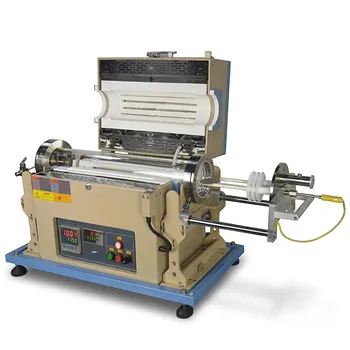
- Chemical Vapor Deposition CVD System Slide PECVD Tube Furnace with Liquid Gasifier PECVD Machine
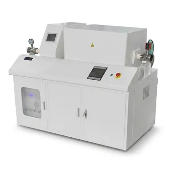
- Inclined Rotary Plasma Enhanced Chemical Vapor Deposition PECVD System for Thin Film Deposition and Nanomaterial Synthesis
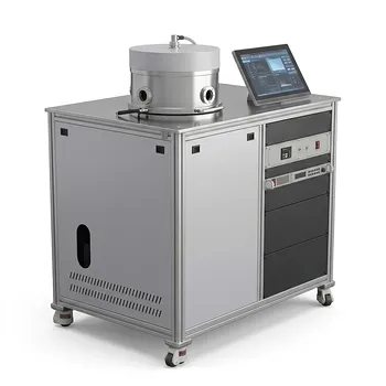
- Radio Frequency Plasma Enhanced Chemical Vapor Deposition RF PECVD System for Laboratory and Industrial Thin Film Growth
- 1200C Max Compact Auto-Sliding PECVD Furnace with 2 Inch Tube and Vacuum Pump
- 1200C Dual Sliding Tube Furnace with Dual Tubes and Flanges for PECVD Processes
People Also Ask
- What are the advantages of PECVD systems for nano flame retardant films? Protect Heat-Sensitive Polymers with Precision
- How does a sliding rail design benefit the CVD process within a furnace ventilation hood? Enhance Control & Quenching
- What is the role of CVD/PECVD systems in the research of optoelectronic materials and functional coatings? Expert Guide
- How does PECVD differ from conventional thermal CVD? Key Advantages of Low-Temperature Deposition for R&D
- What role do by-product desorption and evacuation play in CVD film quality? Key Factors for High-Purity Films

Tech Team · ThermUnits
Last updated on Apr 14, 2026
Related Products
Chemical Vapor Deposition CVD System Slide PECVD Tube Furnace with Liquid Gasifier PECVD Machine
Inclined Rotary Plasma Enhanced Chemical Vapor Deposition PECVD System for Thin Film Deposition and Nanomaterial Synthesis
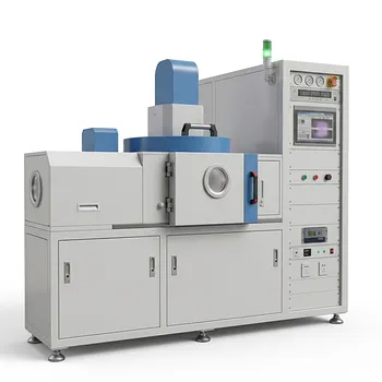
Radio Frequency Plasma Enhanced Chemical Vapor Deposition RF PECVD System for Laboratory and Industrial Thin Film Growth
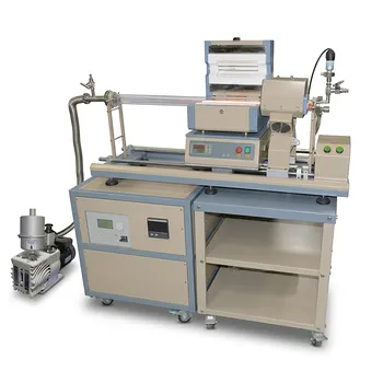
1200C Max Compact Auto-Sliding PECVD Furnace with 2 Inch Tube and Vacuum Pump
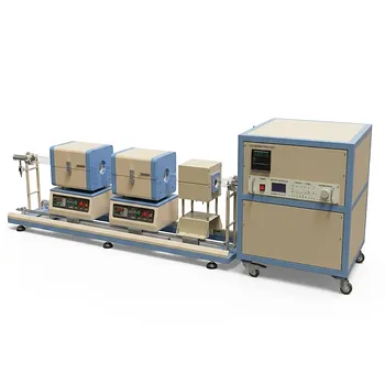
1200C Dual Sliding Tube Furnace with Dual Tubes and Flanges for PECVD Processes
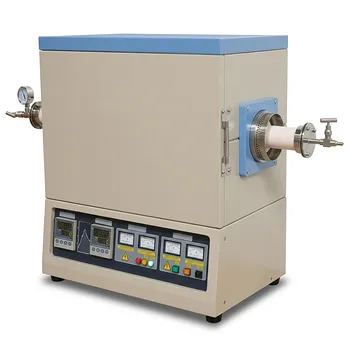
High Temperature 1700C Dual Zone Tube Furnace for Material Science and Industrial Chemical Vapor Deposition Research
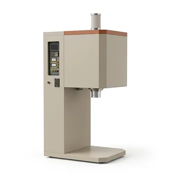
Vertical Openable Tube Furnace 0-1700c High Temperature Laboratory System for CVD and Vacuum Heat Treatment
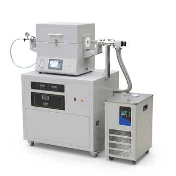
Split Chamber CVD Tube Furnace with Vacuum Station Chemical Vapor Deposition System Machine
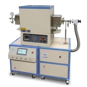
High Temperature 1700C Tube Furnace with High Vacuum Turbomolecular Pump System and Multi Channel Mass Flow Controller Gas Mixer
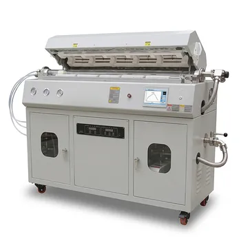
Multi Heating Zones CVD Tube Furnace System for Precision Chemical Vapor Deposition and Advanced Material Synthesis
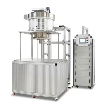
915MHz MPCVD Diamond Machine Microwave Plasma Chemical Vapor Deposition System Reactor
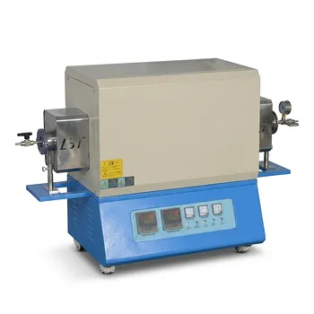
High Temperature Dual Zone Vacuum Tube Furnace for Material Research and CVD Processing
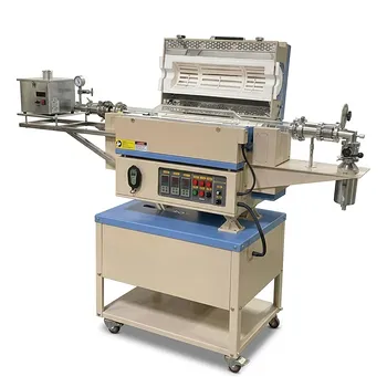
5 Inch Rotary Tube Furnace with Automatic Feeding and Receiving System 1200C Three Zone CVD Powder Processing
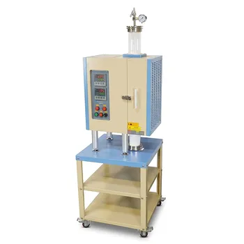
1100°C Dual Zone Split Vertical Tube Furnace with 4 Inch Quartz Tube and Vacuum Sealing Flanges
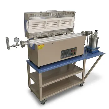
5 Inch Two Zone Rotary Tube Furnace 1100C for Powder CVD and Material Synthesis
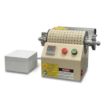
1000C Mini Tube Furnace with 20mm Quartz Tube and Vacuum Flanges for Material Science Research and Controlled Atmosphere Small Sample Processing
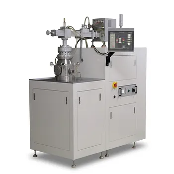
Cylindrical Resonator MPCVD Machine System for Microwave Plasma Chemical Vapor Deposition and Lab Diamond Growth
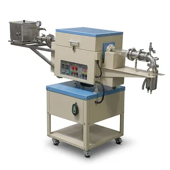
Two Zone Rotary CVD Furnace with Automatic Feeding and Receiving System for Powder Processing
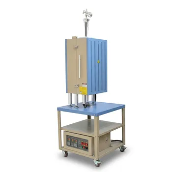
1200C Three Zone Vertical Tube Furnace with 2 Inch Quartz Tube and Vacuum Flanges